
How Data Acquisition Gateway Market Shapes Intelligent Semiconductor Infrastructure?
Data Acquisition Gateway Market is becoming a critical bridge between physical semiconductor-enabled systems and digital intelligence layers. At its core, a data acquisition gateway aggregates signals from sensors, converts analog inputs into digital streams, and transmits structured data to processing units or cloud platforms.
In semiconductor environments, these gateways are no longer passive intermediaries; they are embedded with microcontrollers, signal processors, and edge AI chips that enable real-time filtering and decision-making.
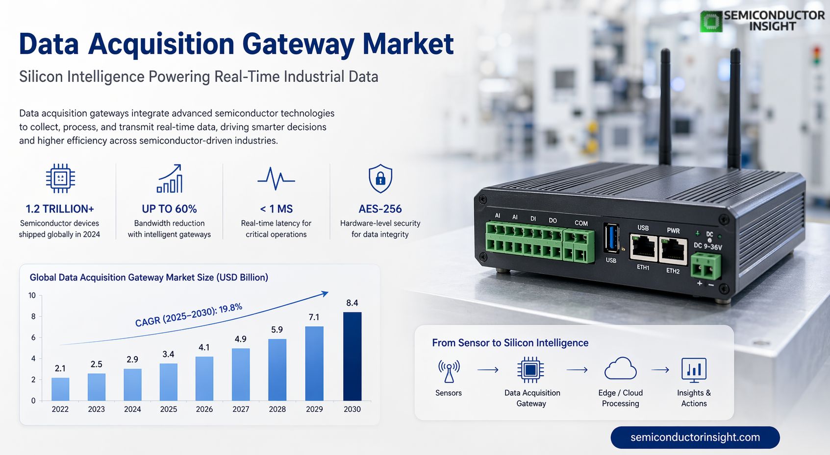
In 2024, global semiconductor device shipments surpassed 1.2 trillion units annually, with a significant portion integrated into sensing and monitoring systems. Each of these devices generates continuous streams of voltage, temperature, pressure, or motion data. Data acquisition gateways act as the first level of intelligence, ensuring that only relevant and structured data reaches higher computing layers, reducing bandwidth usage by up to 40–60% in industrial deployments.
Semiconductor Integration inside Data Acquisition Gateways
- Modern gateways are deeply rooted in semiconductor innovation.
- They rely on mixed-signal integrated circuits that combine analog-to-digital converters (ADCs), digital signal processors (DSPs), and communication interfaces on a single chip.
- High-resolution ADCs, often operating at 16-bit to 24-bit precision, allow accurate capture of minute signal variations in applications such as wafer fabrication monitoring or power electronics testing.
- Edge processing chips within gateways now operate at frequencies exceeding 1 GHz while maintaining power consumption below 5 watts in many industrial modules.
- This balance is achieved through advanced semiconductor nodes such as 7nm and 12nm architectures.
- Additionally, the inclusion of embedded memory ranging from 512 MB to 4 GB allows temporary data buffering and pre-processing before transmission.
Data Flow Architecture from Sensor to Silicon Intelligence
In semiconductor-driven environments, data acquisition gateways are positioned between sensor arrays and centralized compute systems. A typical semiconductor fabrication facility can deploy over 50,000 sensors across equipment such as lithography machines, etchers, and deposition systems. Each sensor may generate data at rates between 1 kHz and 10 kHz, resulting in massive real-time data volumes.
Gateways manage this complexity by implementing multi-protocol communication standards such as SPI, I2C, Modbus, and industrial Ethernet. Data compression algorithms embedded at the silicon level reduce transmission loads, while time-sensitive networking ensures latency remains below 1 millisecond in critical operations. This architecture is essential for maintaining yield rates in semiconductor manufacturing, where even microsecond delays can impact production quality.
For additional report info, feel free to view our most recent edition: https://semiconductorinsight.com/report/data-acquisition-gateway-market/
Strengthening Process Reliability for Improved Fabrication Results
Data acquisition gateways are directly influencing semiconductor yield improvement. In advanced fabs, where wafer defect rates must remain below 0.1%, gateways enable continuous monitoring of environmental variables such as humidity, vibration, and chemical concentrations. For example, maintaining cleanroom particle counts below 100 particles per cubic meter is essential for sub-10nm fabrication processes.
Gateways equipped with real-time analytics can detect anomalies instantly and trigger corrective actions. This reduces downtime and prevents batch-level defects. Some facilities report a reduction of up to 15% in process interruptions after deploying intelligent data acquisition systems.
Chip-Level Signals inside Gateways
- Edge AI in MCUs is the dominant silicon trend driving next-gen gateway designs in 2026, per IoT Analytics State of Enterprise IoT report
- RISC-V architecture gaining momentum in gateway SoC designs lower licensing cost vs. ARM-based platforms
- Qualcomm Snapdragon-class edge AI chips expanding beyond automotive into industrial gateway form factors
- US CHIPS Act semiconductor investment reshaping domestic gateway chip supply chains through 2026
- Siemens Tessent AnalogTest (September 2025): first automated test gen for analog ICs, directly relevant to DAQ signal chain verification
Energy Efficiency and Thermal Constraints in Semiconductor Gateways
Energy efficiency is a critical consideration in gateway design. Semiconductor components used in gateways must operate reliably in environments where temperatures can range from -40°C to 85°C. Power consumption optimization is achieved through low-power semiconductor designs, including FinFET and FD-SOI technologies.
Typical industrial gateways consume between 3W and 15W, depending on processing requirements. Passive cooling solutions are often preferred to avoid mechanical failures, making thermal design a key aspect of semiconductor integration.
Protocol Transition Pressure in Semiconductor Fabs
- Semiconductor fabs are currently balancing the continued use of legacy communication protocols with the growing adoption of modern industrial standards. Older systems such as Modbus, SECS-I, and PROFIBUS remain active in many facilities, especially in brownfield environments and older fabs, but they increasingly depend on protocol gateways to connect with newer platforms and support migration toward Ethernet-based and cloud-ready architectures.
- At the same time, modern protocols are gaining strong momentum across semiconductor manufacturing operations. OPC UA PubSub over MQTT is emerging as the preferred northbound standard for cloud-connected fabs, while SEMI EDA supports high-bandwidth equipment data collection for AI-driven fault detection. In parallel, TSN is enabling highly precise synchronization across data acquisition nodes, which is essential for accurate wafer process alignment and advanced smart factory control.
Hardware Security and Data Integrity at the Silicon Level
Security is becoming a foundational requirement in the Data Acquisition Gateway Market. Semiconductor-based hardware security modules (HSMs) are now embedded within gateways to ensure data integrity and prevent unauthorized access. Encryption standards such as AES-256 are implemented directly at the chip level, enabling secure data transmission without compromising performance.
Secure boot mechanisms and tamper detection circuits further enhance reliability, especially in critical semiconductor applications such as defence electronics and healthcare devices.
Semiconductor Supply Chain Influence on Gateway Availability
The availability of data acquisition gateways is closely tied to semiconductor supply chains. During the global chip shortage between 2020 and 2022, lead times for certain microcontrollers extended beyond 40 weeks. This impacted gateway production and deployment timelines across industries.
As semiconductor fabrication capacity expands, with new fabs capable of producing over 100,000 wafers per month, the supply of critical components for gateways is stabilizing. This is expected to support the continued expansion of the market.

Comments (0)