
How Big Is the MCP Memory Market in 2026? Key Integration Facts
MCP memory continues to play a pivotal role in semiconductor design by combining multiple memory types into compact, high-performance packages that power everything from everyday smartphones to advanced industrial systems.
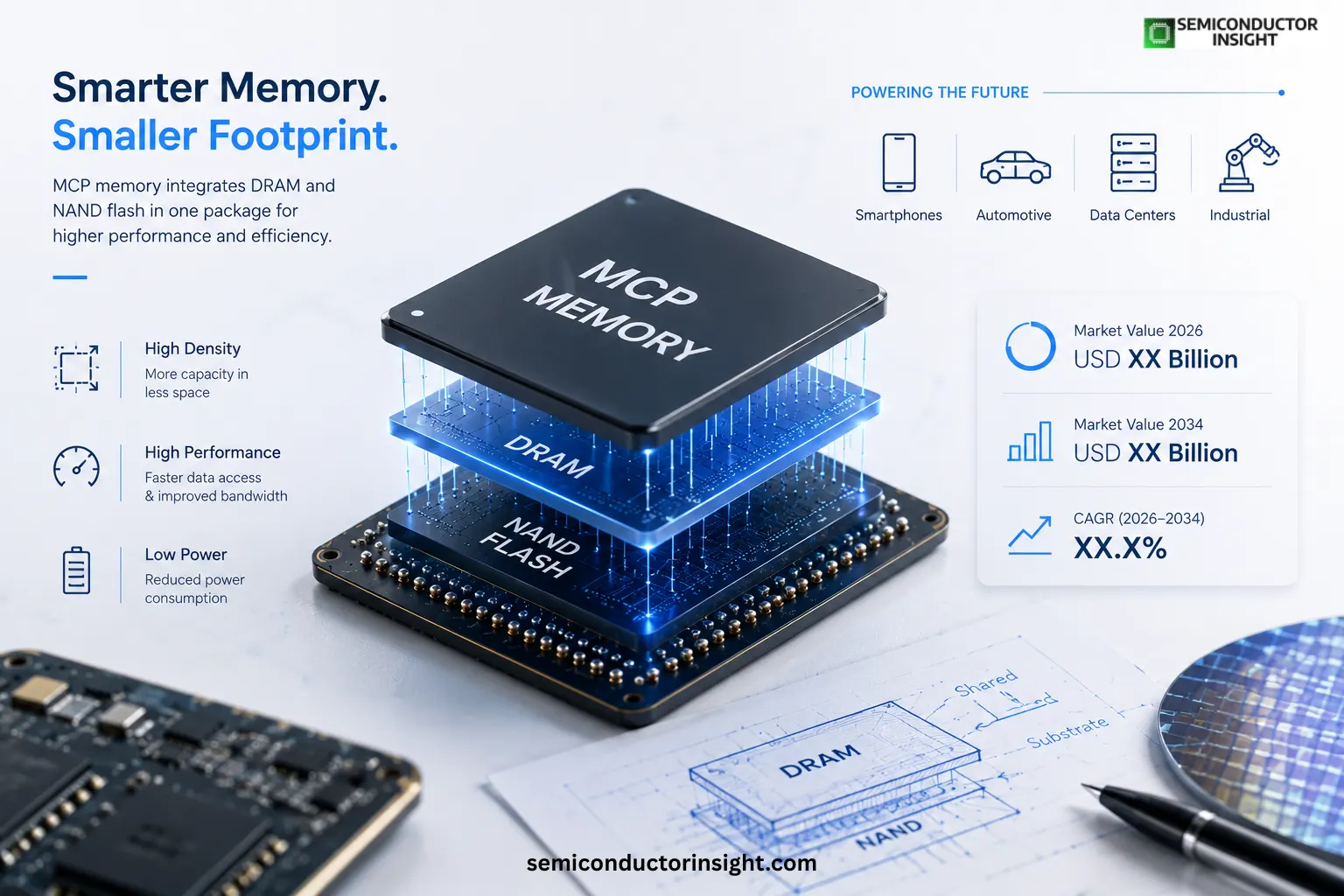
These solutions stack dies vertically or side-by-side on a shared substrate, delivering denser storage and faster data access while minimizing board space and power draw. Manufacturers like Samsung and Micron have long refined these approaches to meet demands for thinner devices with greater capabilities.
Understanding Multi-Chip Packaging in Semiconductors
- Multi-chip packaging, commonly referred to as MCP in the memory space, integrates two or more semiconductor dies such as NAND flash and DRAM into a single unified enclosure.
- This creates what appears externally as one component but internally houses layered or parallel memory elements.
- The technology emerged prominently with mobile devices needing combined code storage and working memory without expanding physical footprints.
- Recent studies and technical resources describe it as treating the assembly like a larger integrated circuit, enabling system-level efficiencies.
- In practice, MCP configurations range from simple dual-die stacks to complex multi-layer setups supporting diverse functions like flash, SRAM, and even logic elements.
Smart Device Ecosystem Integration with MCP Memory
Leading electronics brands rely on MCP memory for seamless operation in connected environments. For example, flagship smartphones utilize these packages to handle high-resolution imaging, multitasking, and always-on features efficiently.
Automotive manufacturers incorporate ruggedized MCP variants for infotainment and advanced driver assistance systems, where space constraints and reliability under vibration are paramount. Viking Technology highlights their use in embedded and military applications, achieving higher density per cubic inch compared to traditional modules.
You can freely browse our most recent updated report to learn more about it before scrolling further: http://semiconductorinsight.com/report/mcp-memory-market/
Current Global Deployments and Real-World Examples
- Ongoing projects worldwide demonstrate MCP memory’s expanding footprint. In the United States, investments under the CHIPS and Science Act support advanced packaging facilities that enhance MCP capabilities for high-bandwidth applications.
- Micron’s expansions in Idaho and New York include facilities focused on memory integration and 3D stacking technologies critical for next-generation MCP solutions.
- One notable effort involves collaboration with universities for research into heterogeneous integration, directly benefiting MCP designs used in AI training hardware.
- Internationally, consumer electronics production in Asia continues scaling MCP adoption for portable devices. Case studies from industry publications show mobile phone memory shipments growing substantially as MCP formats allow doubling capacity within the same footprint, supporting features like 5G connectivity and enhanced graphics.
- Government initiatives promoting domestic semiconductor ecosystems further accelerate these integrations in secure communications and computing infrastructure.
Performance Metrics from Authorized Technical Sources
Public data from semiconductor producers indicates MCP solutions deliver significant density gains. For instance, certain DDR4 MCP configurations provide 8GB to 16GB capacities in compact X32 or X72 widths, optimized for SWaP (Size, Weight, and Power) constrained systems. These metrics translate to lower motherboard complexity and reduced routing challenges in end products.
- Emerging Applications in High-Performance Computing
- Beyond consumer gadgets, MCP memory supports data center and edge computing needs.
- Stacked configurations help manage thermal loads and bandwidth requirements in servers handling massive parallel processing.
- Recent facility announcements emphasize advanced test and packaging lines dedicated to such memory technologies, aligning with broader goals of supply chain resilience.
- Material and Design Innovations Driving Progress
- Developments focus on improved substrates, through-silicon vias, and better thermal management within packages.
- These advancements allow higher layer counts and mixed memory types without compromising speed or longevity.
- Technical articles note how MCP technology first addressed 2.5G and 3G phone requirements and has since evolved to underpin modern 5G and AI edge devices.
- Integration with Broader Semiconductor Ecosystems
- MCP memory fits into larger heterogeneous systems where memory, processors, and sensors coexist efficiently.
- This synergy proves valuable in automotive dashboards, medical devices, and industrial controls, where reliable data handling in limited spaces is essential.
- DARPA and NIST-backed programs explore next-generation packaging that builds upon MCP principles for even more sophisticated 3D integrations.
Sustainability and Efficiency Considerations
Efficient packaging like MCP contributes to lower overall energy consumption in devices by reducing interconnect lengths and parasitic losses. As global efforts prioritize sustainable electronics, these compact solutions help manufacturers meet efficiency targets while delivering more functionality per unit.
Expansions in U.S. facilities under federal support aim to localize such production, fostering innovation in eco-friendly materials and processes.
The MCP memory domain reflects the semiconductor industry’s push toward greater integration and performance in ever-smaller forms. Through real-world deployments in consumer, automotive, and computing sectors, these packages enable the devices and systems shaping daily life and future technologies. Continued advancements, supported by public-private initiatives, ensure their relevance as demands for speed, capacity, and efficiency grow.

Comments (0)