
How Are Vacuum Sensors Powering Advanced Semiconductor Processes in 2026?
Semiconductor manufacturing operates in environments where even microscopic pressure variations can derail entire production runs. Vacuum sensors stand as silent guardians, delivering the exact measurements needed to sustain ultra-clean chambers during critical steps like chemical vapor deposition, etching, and wafer handling. These devices track pressures across wide ranges, from rough vacuum down to high and ultra-high levels, ensuring processes remain stable and contamination-free.
In fabs worldwide, operators rely on these sensors to maintain conditions that allow atoms to deposit precisely onto silicon wafers. For instance, during atomic layer deposition (ALD), a custom vacuum sensor with ultra-high purity construction helps control the delicate balance in new-generation equipment, preventing particle intrusion and enabling thinner, more uniform layers essential for smaller nodes.
Inside the Vacuum Ecosystem Powering Chip Innovation
- Vacuum technology forms the backbone of semiconductor equipment. Dry vacuum pumps, paired with precise sensors, evacuate toxic fumes and maintain chamber integrity beneath production floors. Recent investments highlight this importance. Under the CHIPS and Science Act, Edwards Vacuum received support for a new manufacturing facility in Genesee County, New York, focused on dry vacuum pumps critical for both advanced and legacy chip production. This project aims to create hundreds of jobs and address previous gaps in domestic supply for semiconductor-grade equipment.
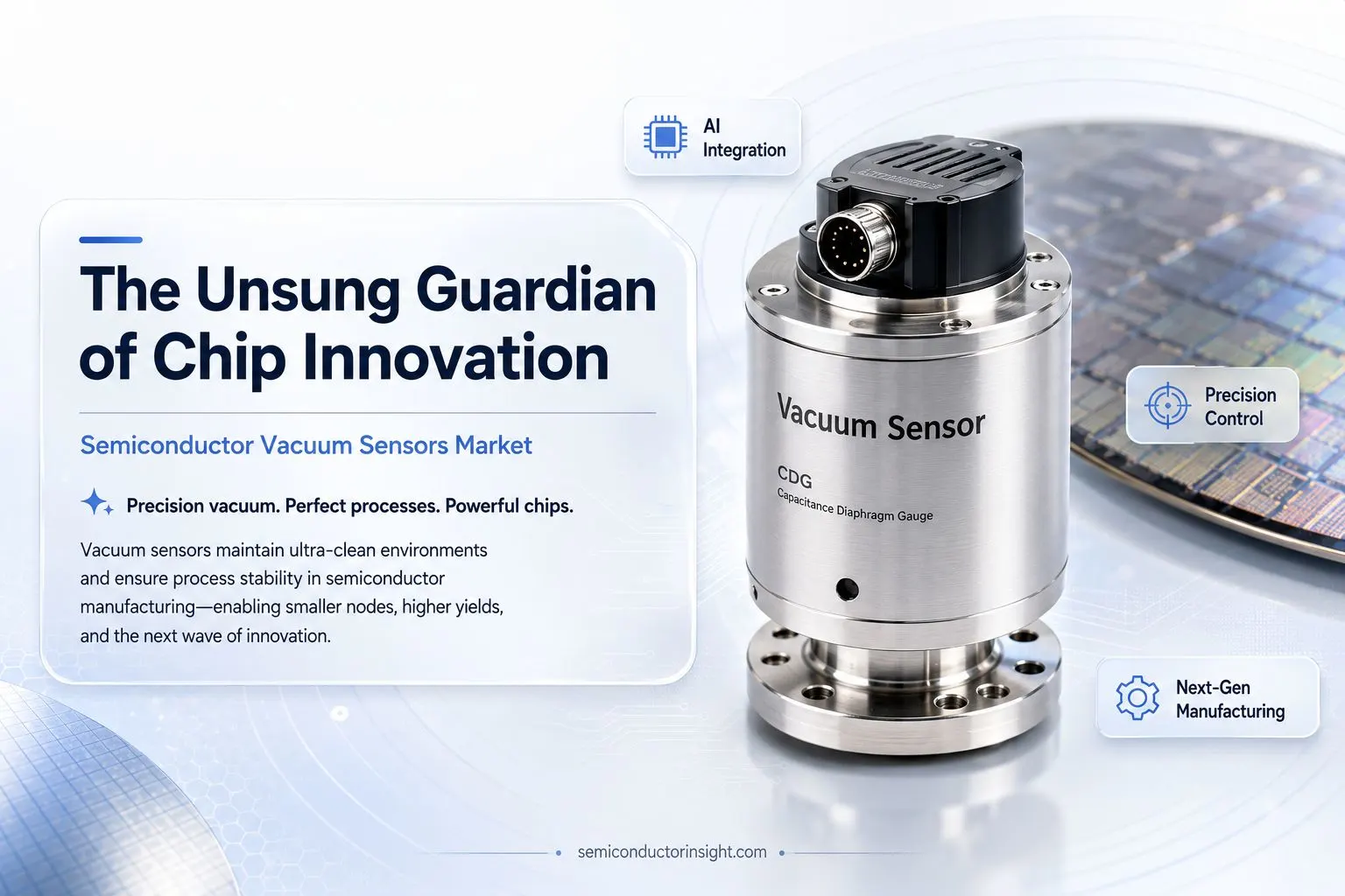
- MEMS (micro-electromechanical systems) approaches are gaining traction for their compact size and integration potential. These tiny sensors, often built using surface or bulk micromachining on silicon wafers, combine mechanical structures with electronics. Pirani gauges, which measure thermal conductivity changes, and capacitance diaphragm gauges (CDGs), which detect diaphragm deflection independently of gas type, serve as workhorses. CDGs offer high accuracy often better than 0.25-0.5% of reading and excel in process monitoring where gas composition varies.
- Recent research explores hybrid designs, such as weak-coupling resonators in MEMS diaphragms, operating in dual modes: mode-localized for medium vacuum sensitivity and resonance for higher accuracy at other ranges. These aim to overcome limitations of single-type sensors, providing broader coverage from 0.1 Pa to 10^5 Pa with improved resolution, vital for load-lock systems and plasma tools.
Real-World Deployments Shaping Global Production Lines
Consider wafer deposition processes where precise vacuum control directly impacts yield. In one application case, a specialized sensor supported ALD advancements by offering both purity and tailored sensitivity, helping manufacturers scale next-generation devices without compromising cleanliness.
Globally, semiconductor expansion drives demand. Facilities in Asia, the US, and Europe integrate these sensors into tools for EUV lithography, which requires extremely low pressures. INFICON, a key player with roots in vacuum instrumentation, supplies gauges, controllers, and residual gas analyzers used across the industry, reporting steady growth tied to fab activity.
Government initiatives like the CHIPS Act further accelerate adoption by funding equipment modernization and R&D, reducing reliance on single geographic sources and enhancing supply chain security.
Spotlight on Top-Performing Vacuum Sensor Solutions
Leading Vacuum Monitoring Technologies for Semiconductor Excellence
Among options, capacitance diaphragm gauges frequently stand out for their reliability in process-critical environments. Models from established providers deliver gas-independent readings with exceptional repeatability, making them standards for etching and deposition tools. For broader coverage, composite systems pairing Pirani elements with CDGs handle transitions from atmosphere to high vacuum effectively.
MEMS innovations, such as thermopile or resonator-based designs, appeal for space-constrained or integrated applications, offering miniaturization while maintaining performance. Selection depends on factors like required range, accuracy needs, and compatibility with corrosive gases common in fabs. Engineers often prioritize sensors with fast response, low drift, and easy integration into control systems for predictive maintenance.
You Can Go Through Our Latest Updated Insights Here: https://semiconductorinsight.com/report/semiconductor-vacuum-sensors-market/
How Miniaturization and Smart Integration Are Transforming Operations?
Advancements in wafer-level vacuum packaging allow sensors to combine with CMOS electronics, creating compact, hermetic modules. Techniques like eutectic bonding or anodic bonding ensure long-term stability in harsh environments.
Digital features, including IoT connectivity for real-time data, enable fabs to optimize uptime and reduce downtime through predictive analytics. Energy-efficient designs in associated pumps and sensors align with sustainability goals, cutting power use in high-volume production.
Navigating the Path Forward in Vacuum Sensing
As nodes shrink below 2nm and new materials enter production, vacuum sensors must evolve for even tighter tolerances. Ongoing work in porous silicon platforms and frequency-modulated thermoelectric sensors points to higher reliability and lower costs.
The interplay between policy support, technological refinement, and fab expansions positions vacuum sensing as a cornerstone of semiconductor progress. From preventing contamination in load locks to enabling precise process control, these unassuming devices keep the industry’s heartbeat steady amid rapid innovation.

Comments (0)