

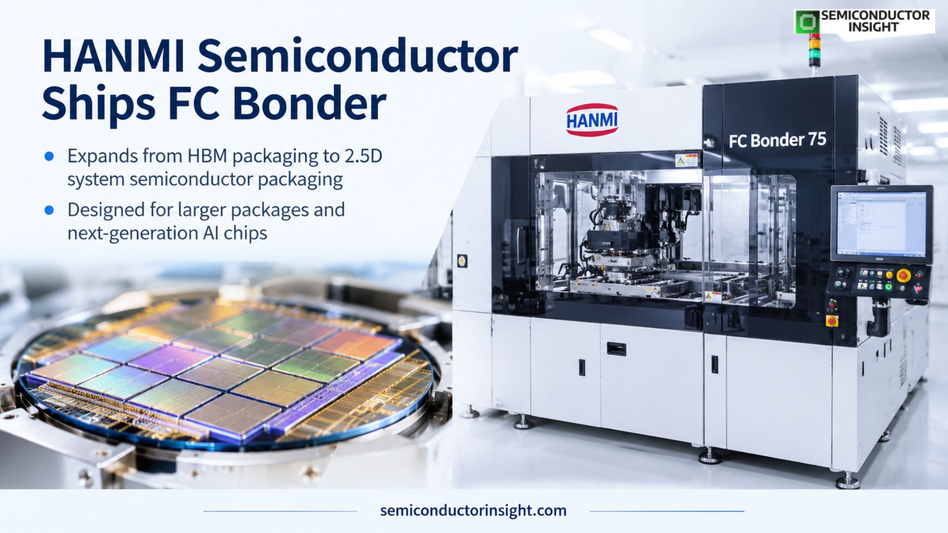
HANMI Semiconductor Ships FC Bonder 75 as AI Packaging Moves Toward Larger 2.5D Architectures
Race to scale AI computing is increasingly shifting from the chip itself to the advanced packaging technologies that connect processors, accelerators and high-bandwidth memory. Against this backdrop, HANMI Semiconductor has shipped the first “FC Bonder 75” to a customer, marking the company’s expansion from its established HBM packaging business into a broader segment of 2.5D system semiconductor packaging.
The new flip-chip bonding platform is designed around the larger package dimensions increasingly required by next-generation AI semiconductors, where multiple high-performance dies must operate together within a tightly integrated package.
A Larger Packaging Footprint for AI Compute
AI accelerators are becoming more complex as computing architectures combine CPUs, GPUs, ASICs and HBM within advanced multi-die packages. As the number and size of integrated components increase, conventional packaging dimensions can become restrictive.
HANMI’s FC Bonder 75 addresses this requirement by supporting 75 mm × 75 mm interposer packages, substantially larger than the conventional 20 mm × 20 mm general-purpose packaging format cited by the company.
The larger bonding area is intended to accommodate ultra-large dies and multiple semiconductor components while enabling the dense interconnections required for advanced AI systems.
Why 2.5D Packaging Is Becoming Strategic?
The move into 2.5D packaging reflects a broader transformation taking place across the semiconductor supply chain.
Instead of relying exclusively on increasingly large monolithic dies, advanced semiconductor architectures can divide computing functions among multiple dies and connect them through an interposer or other advanced integration technologies. This approach has become particularly important for AI systems, where processors must exchange enormous quantities of data with HBM at high speed.
Flip-chip bonding plays a critical role in this architecture. The semiconductor die is positioned face down so that conductive bumps connect directly with the interposer, creating short electrical pathways and high-density interconnections.
As AI system complexity increases, equipment capable of handling larger package formats is becoming increasingly relevant to foundries and outsourced semiconductor assembly and test (OSAT) providers.
- HANMI Semiconductor has historically built significant capabilities around semiconductor packaging equipment, particularly technologies associated with HBM.
- The FC Bonder 75 represents a strategic extension of that portfolio.
- The company has also introduced several other 2.5D packaging systems during 2026, including the FC Bonder 3.5, 2.5D TC Bonder 40 C2S and 2.5D TC Bonder 40 C2W, while preparing the 2.5D TC Bonder 120.
- Together, these products indicate a move toward a wider equipment portfolio capable of supporting different advanced packaging architectures, package dimensions and bonding requirements.
AI Packaging Competition Is Expanding
The technology landscape surrounding 2.5D and 3D packaging is becoming increasingly competitive as semiconductor manufacturers seek ways to integrate more computing performance within a single system.
TSMC’s CoWoS has become a prominent example of 2.5D integration for AI processors, while the company is also developing approaches such as Chip on Panel on Substrate (CoPoS) and 3D System on Integrated Chips (3D-SoIC).
Meanwhile, Intel’s EMIB-T technology is being applied to advanced ASIC architectures, including applications associated with major U.S. technology companies.
These developments are increasing the importance of the equipment ecosystem behind advanced packaging. Packaging equipment suppliers are therefore becoming increasingly connected to the expansion of AI compute infrastructure.
The U.S. Becomes an Important Expansion Point
HANMI’s equipment expansion is also being accompanied by a stronger push into the U.S. semiconductor ecosystem.
The company plans to establish HANMI USA, with operations expected to support major technology companies, foundries, OSAT companies and memory manufacturers in the U.S. The company expects its U.S. activities to ramp up toward 2028.
This geographical expansion could position HANMI closer to customers investing heavily in AI processors, advanced packaging and memory technologies.
For equipment manufacturers, proximity to major semiconductor customers is becoming increasingly important as advanced packaging moves from a specialized manufacturing capability toward a core part of AI chip production.
The significance of the FC Bonder 75 extends beyond the launch of another bonding machine.
- As AI chips become larger and more heterogeneous, packaging dimensions, interconnect density, thermal management and die-to-die communication are increasingly influencing system-level performance.
- This is creating a new competitive layer in the semiconductor industry one where the ability to manufacture and assemble complex multi-die systems can be just as strategically important as designing the individual processor.
- HANMI’s latest shipment therefore reflects a broader industry transition: AI semiconductor innovation is moving deeper into the packaging stack.
With its FC Bonder 75 and expanding 2.5D equipment portfolio, HANMI Semiconductor is positioning itself to participate in that transition as chipmakers and packaging providers prepare for increasingly large and complex AI systems.
As AI architectures scale, the next semiconductor bottleneck may not simply be transistor density it may be the ability to connect more chips, more memory and more computing power inside a single package.
Access the Latest Insights from Our Newly Released Study: https://semiconductorinsight.com/report/semiconductor-packaging-materials-market/

Comments (0)