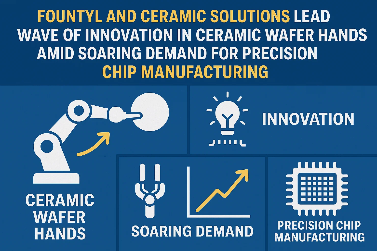
Fountyl and Ceramic Solutions Lead Wave of Innovation in Ceramic Wafer Hands Amid Soaring Demand for Precision Chip Manufacturing
The semiconductor industry is experiencing an era of extraordinary transformation. As the demand for faster, smaller, and more efficient chips intensifies, so does the need for innovations in supporting technologies. One such overlooked, yet critically important innovation lies in ceramic wafer hands, also referred to as ceramic end-effectors or robotic wafer handling arms. These advanced tools, often made from high-purity alumina or silicon carbide (SiC), are vital to achieving the precision and cleanliness required in modern semiconductor fabrication.
The Ceramic Wafer Hands Market, valued at US$ 127.4 million in 2024, is forecast to grow at a CAGR of 8.0%, reaching US$ 218.6 million by 2032. This impressive trajectory reflects the rising demand for highly automated, contamination-free semiconductor manufacturing processes, especially as the industry transitions to 300mm and even 450mm wafers and EUV lithography.
Access Your Free Sample Report- Ceramic Wafer Hands Market
Why Ceramic Wafer Hands Matter
The Unsung Heroes of Chipmaking
While silicon chips are the stars of the show, the tools that help handle them silently operate behind the scenes—wafer by wafer, layer by layer. Ceramic wafer hands, often attached to robotic systems, are designed to pick, place, and transport silicon wafers during fabrication with extreme precision and zero contamination.
These tools must exhibit:
- Thermal stability to endure high-temperature processes (>1000°C)
- Chemical resistance for use in corrosive etching or cleaning environments
- Mechanical strength and stiffness to prevent deflection
- Ultra-smooth, non-contaminating surfaces
Why Ceramics?
Materials like 99.7% alumina and SiC ceramics offer several advantages over traditional materials like stainless steel or aluminum:
- Lower particle generation
- Higher purity and lower outgassing
- Minimal wear and longer lifespan
- Better dimensional accuracy
With chip architectures growing increasingly complex (e.g., 3D NAND, FinFET), even a micron-level misalignment or contaminant can compromise the entire process. Ceramic wafer hands help eliminate these risks.
Market Dynamics and Forecast (2025–2032)
The global ceramic wafer hands market, which stood at US$ 127.4 million in 2024, is poised to grow steadily over the next decade. This growth is being driven by:
- Rising investments in EUV lithography, which requires extreme cleanliness
- Expansion of 300mm wafer fabs, especially in Asia-Pacific
- Surge in foundry outsourcing by fabless chipmakers
- High demand for advanced packaging and heterogeneous integration
Technological Advancements
- Custom Ceramic End-Effectors: Fountyl Technologies’ Innovation
Fountyl Technologies has made headlines with its custom ceramic end-effectors, tailored to handle a wide range of wafer sizes, shapes, and weights. These end-effectors are lightweight, anti-static, and optimized for vacuum and atmospheric pressure environments—making them ideal for next-gen fabs.
“Customization is the new standard. As wafers become more diverse, we need tools that are designed with specific mechanical and thermal parameters in mind.” – Fountyl R&D Spokesperson
Key Innovations:
- Tailored slots for multi-size wafers (100mm–450mm)
- Optional sensor integration for feedback control
- Surface texturing to prevent sticking or slipping
- High-Purity 99.7% Alumina Ceramic Plates for Polishing and Cleaning
Recent reports confirm widespread adoption of 99.7% alumina ceramic polishing plates in wafer cleaning and CMP (chemical mechanical planarization). These polishing plates are thermally stable up to 1600 °C and maintain surface uniformity even after repeated use.
Applications:
- Wet chemical processing
- Wafer bevel polishing
- Substrate conditioning in CMP lines
Benefits:
- Reduced wafer edge chipping
- Lower particle generation
- Increased yield rates in CMP
- Bernoulli-Based Robotic Arms from Ceramic Solutions (Italy)
Ceramic Solutions has introduced Bernoulli suction-based wafer handling arms made from alumina and SiC ceramics. These arms allow non-contact wafer transfer, minimizing wafer warpage or scratching—critical for ultra-thin or delicate wafers.
Highlights:
- High resistance to thermal shock
- Optimized for vacuum and clean-room integration
- Modular design supports quick retooling
- Nanotech-Enhanced Coatings for 300mm Wafers
New research from East Asia suggests the use of nano-engineered ceramic coatings that resist corrosion while maintaining a friction-free surface. These coatings are being tested for use in EUV fabs where even sub-nanometer particles can disrupt lithography.
Download Sample Report PDF- Ceramic Wafer Hands Market
Application Landscape
Ceramic wafer hands find applications across a variety of semiconductor processes:
- Front-End Wafer Fabrication
- Lithography
- Etching
- Ion implantation
- CMP
- Back-End Processing
- Die singulation
- Advanced packaging
- Wafer-level testing
- Wafer Transfer and Sorting
- FOUP (Front Opening Unified Pods)
- Vacuum robotic arms
- Air-floating transfer platforms
- Cleanroom Automation Systems
- Integrated with AGVs and robotic arms
- Contamination-controlled environment
Key Benefits Driving Adoption
Here are the major benefits making ceramic wafer hands indispensable:
- Contamination-Free Handling: Their chemical inertness ensures no outgassing or particle generation.
- Precision Movement: Dimensional stability ensures accurate placement even under thermal/mechanical stress.
- Longevity: Ceramics outlast metal alternatives by 2x–3x in abrasive or corrosive settings.
- High Customizability: End-effectors can be engineered for specific wafer types or process lines.
Regional Analysis
Asia-Pacific: The Growth Engine
Countries like China, Taiwan, South Korea, and Japan are investing billions into semiconductor self-sufficiency. This includes building new 300mm fabs, which are entirely dependent on precision wafer handling systems.
United States: Innovation Hub
The U.S. remains at the forefront of material innovation. Firms are experimenting with ceramic-carbon hybrids and ultralight foamed ceramics for higher robotic throughput.
Europe: Specialized Applications
European players are focusing on MEMS, automotive chips, and optics, where wafer fragility demands superior handling precision.
Challenges & Limitations
Despite rapid growth, the industry faces several hurdles:
- High Cost of Raw Materials: Ultra-pure ceramics are expensive to manufacture.
- Complex Manufacturing Process: Precision machining and sintering increase lead times.
- Integration Barriers: Compatibility with legacy robotic systems can be difficult.
- Supply Chain Disruptions: Global political instability affects ceramic supply lines.
However, technological innovation and rising chip complexity are expected to mitigate these barriers over time.
The Future of Ceramic Wafer Hands
Looking ahead, the ceramic wafer hand market will likely evolve in the following ways:
- Smart End-Effectors
Expect built-in sensors for force, temperature, and electrostatic discharge monitoring—enabling closed-loop process control.
- AI-Powered Robotic Handling
Integration with AI algorithms will help optimize wafer movement paths and reduce human intervention.
- 450mm Wafer Compatibility
With exploratory fabs testing 450mm wafers, ceramic handling systems will require structural redesigns to support the larger, heavier substrates.
- Hybrid Materials
Combining ceramics with carbon composites or metallic reinforcements to balance strength, weight, and cost.
Click Here To Download Full Sample Report- Ceramic Wafer Hands Market
Ceramic wafer hands may be invisible to the consumer, but they are pivotal in the production of every microchip powering modern life—from smartphones and laptops to cars and satellites. Their ability to handle wafers with precision, purity, and durability makes them a cornerstone technology in semiconductor fabrication.
With the industry’s transition to more advanced manufacturing nodes, greater automation, and stringent cleanliness standards, ceramic wafer hands are no longer just components—they’re enablers of the next chipmaking revolution.
As we approach 2032, stakeholders who invest in ceramic wafer handling innovations will be best positioned to lead in yield, throughput, and performance in an increasingly competitive semiconductor market.
Comments (0)