
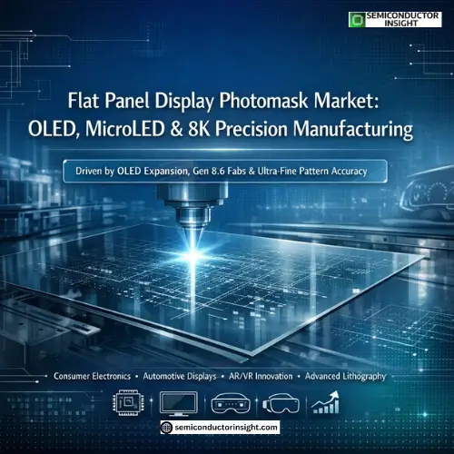
Flat Panel Display Photomask Market Analysis: Advanced Mask Technologies Reshaping Display Manufacturing
In the rapidly advancing semiconductor and display manufacturing landscape, flat panel display photomasks have become an essential yet often overlooked component. As display technologies transition from traditional LCD panels to OLED and MicroLED architectures, the demand for highly precise photomasks is intensifying. These masks serve as the blueprint that transfers intricate circuit patterns onto glass substrates, directly influencing display resolution, brightness, and performance efficiency.
The flat panel display photomask market is witnessing accelerated momentum driven by expanding consumer electronics production, increasing large-screen television demand, and rapid innovation in automotive and smart device displays. What once functioned as a supporting manufacturing tool has now emerged as a critical manufacturing enabler in next-generation display ecosystems.
The Technology Backbone of Advanced Displays
Photomasks used in flat panel displays differ from traditional semiconductor masks in terms of size, substrate requirements, and exposure technologies. Large-area masks are required for Gen 8, Gen 10.5, and higher fabrication facilities, especially for large televisions and commercial display panels.
As OLED and AMOLED panels gain market share in smartphones and premium TVs, mask precision requirements are tightening. Fine metal mask (FMM) technologies, phase-shift masks, and high-resolution patterning techniques are becoming integral. The migration toward 4K and 8K resolution displays demands exceptional alignment accuracy, reinforcing the need for ultra-fine pattern accuracy.
Additionally, increasing panel complexity such as foldable displays and flexible substrates has expanded engineering requirements, pushing photomask manufacturers toward advanced inspection and repair technologies.
Market Expansion Fuelled by Consumer Electronics & Automotive Demand
Global display panel production continues to scale, particularly across Asia-Pacific manufacturing hubs including China, South Korea, and Taiwan. Rising investments in OLED fabrication plants are directly strengthening photomask procurement volumes.
Smartphones remain a primary growth engine, with OLED penetration exceeding half of premium handset shipments globally. Meanwhile, the automotive sector is emerging as a high-value contributor, as digital dashboards, infotainment panels, and heads-up displays become standard features in modern vehicles.
The integration of MicroLED in augmented reality (AR) and virtual reality (VR) devices further widens the opportunity landscape. These emerging applications require high-density circuit layouts, making photomask sophistication indispensable.
Capital Investment Trends & Fabrication Upgrades
Display manufacturers are investing heavily in upgrading fabrication lines to accommodate next-generation panels. New Gen 8.6 OLED fabs and large-size TV production facilities require photomasks capable of supporting large glass substrates while maintaining micron-level accuracy.
Capital expenditure in display fabs is strongly correlated with photomask demand cycles. As new facilities are commissioned, mask sets are required at every stage of product development from pilot production to mass manufacturing.
Moreover, as yield optimization becomes central to cost efficiency, advanced mask inspection and repair solutions are gaining strategic importance. Reduced defect density directly improves panel yields, making photomask quality a board-level priority for display producers.
At Last before Ending, Don’t Forget to Browse Our Recent Exclusive Report for Detailed Insights:
http://semiconductorinsight.com/report/global-flat-panel-display-photomask-market/
Innovation Frontiers: MicroLED, Foldable & Beyond
- MicroLED technology represents one of the most promising frontiers in display manufacturing. MicroLED panels, in contrast to OLED, necessitate intricate mass transfer and patterning procedures, which puts further strain on photomask accuracy.
- Foldable smartphones and rollable televisions introduce new engineering variables, including substrate flexibility and pixel uniformity challenges. Photomasks tailored for these applications must maintain exceptional dimensional stability under varying processing conditions.
Looking ahead, the convergence of semiconductor and display manufacturing technologies may redefine mask architecture altogether. The increasing overlap between logic chip miniaturization and display pixel density highlights the strategic role of next-generation lithography solutions in shaping the future of visual technology.
Flat panel display photomask market stands at the intersection of semiconductor precision and consumer electronics innovation. As panel makers pursue higher resolutions, energy efficiency, and design flexibility, photomask technologies will continue to evolve in parallel.
In an era where every pixel matters, photomasks remain the invisible architects of display excellence quietly shaping the clarity, color, and performance of the screens that power modern life.

Comments (0)