
Ferrite vs. Ceramic Cores across the Wire Wound Chip Reactors Market
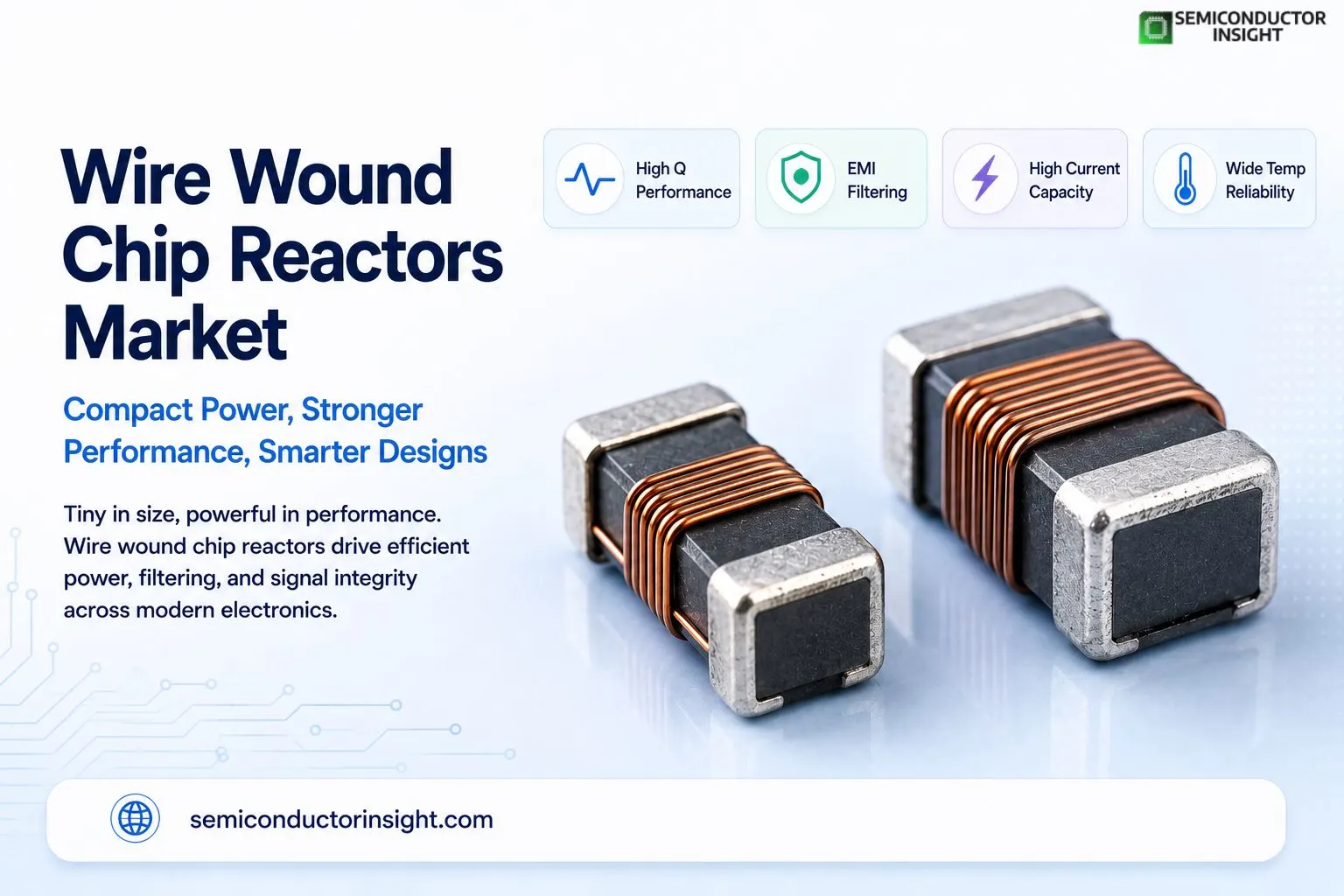
A wire wound chip reactor starts as fine insulated copper wire wrapped around a ceramic or ferrite core and finished with solderable terminations.
The finished part measures only a few millimeters yet creates a controlled magnetic field that resists sudden changes in current. Designers place these components on power rails, RF signal paths, and filter networks where space is measured in tenths of a millimeter.
Winding Geometry That Raises Q and Self-Resonance
Because the wire sits in a single layer or tightly controlled spiral, inter-winding capacitance stays lower than in multilayer chip inductors. The result is higher quality factor values, often in the range of 20 to 80 at 100 MHz, and a higher self-resonant frequency.
That combination lets the component remain inductive at frequencies where other constructions begin to behave like capacitors. Typical inductance values run from 1 nH in the smallest 0402 packages up to several hundred nanohenries in slightly larger outlines such as 0805.
Core Material Shapes Everyday Performance
Ceramic cores keep losses low at radio frequencies and support tight inductance tolerance. Ferrite cores raise permeability and therefore deliver higher inductance or impedance in the same footprint, which suits broadband choke and EMI filtering work. Recent ferrite-core wirewound parts in 0402 size, for example, provide more impedance across a wide frequency band than thin-film alternatives of the same outline. Designers match the core to the job rather than forcing one material into every circuit.
- Current Capacity on a Tiny Footprint
- Thicker wire and careful winding allow some surface-mount wire wound parts to handle continuous currents above 1 A while still fitting standard pick-and-place equipment.
- One published family covers 1 nH to 820 nH with a maximum DC current rating of 1.4 A.
- Heat leaves the component mainly through the terminations and the copper planes of the printed circuit board, so layout becomes part of the thermal design.
- Filtering Noise Before It Spreads
- In switching power supplies the reactor sits in series with the input or output and blocks high-frequency ripple. In RF front ends it forms part of matching networks or bias tees.
- In digital boards it isolates noisy power domains from sensitive analog sections. Because the magnetic field is confined by the core and the small physical size, coupling to nearby traces remains manageable when the board layout follows basic separation rules.
- Assembly and Inspection Realities
- Modern production lines wind the wire under machine control, mold or encapsulate the body, and apply terminations that survive reflow soldering.
- Automated optical inspection checks for missing turns, wire damage, or termination defects before the parts leave the factory.
- These process steps keep the electrical parameters repeatable enough for high-volume consumer, industrial, and automotive assemblies.
You can freely browse our most recent updated report to learn more about it before scrolling further: https://semiconductorinsight.com/report/wire-wound-chip-reactors-market/
Temperature and Reliability Expectations
Automotive and industrial grades must hold inductance and resistance within specified limits across temperature ranges that can reach from -40 °C to +125 °C or higher. The same parts often appear in communication modules and power-management circuits that ride along with the broader semiconductor supply chain. Investments under the CHIPS and Science Act focus mainly on active devices and advanced packaging, yet the passive components that sit beside those chips continue to be specified, purchased, and placed in the same design cycles.
The wire wound chip reactor remains a quiet but essential element. Its construction is simple in concept, yet the combination of controlled winding, chosen core, and surface-mount outline lets engineers manage current, filter noise, and preserve signal integrity on boards that grow denser every year.

Comments (0)