
Fast Charging Breakthroughs Driven by GaN Half-Bridge ICs Market Innovation
GaN Half-Bridge ICs Market is quietly reshaping how modern electronics consume and manage energy. Gallium Nitride has stepped beyond being a niche material and is now deeply embedded in high-performance switching devices.
What makes this shift fascinating is not just efficiency gains but how entire system architectures are being reimagined. Engineers are no longer designing around silicon limitations but instead exploring compact, high-frequency layouts that were previously impractical.
Advanced Power Conversion Strategies Using GaN Switching Structures
A half-bridge IC essentially integrates two switching devices into a single configuration, enabling efficient power conversion in applications like inverters, motor drives, and DC-DC converters.
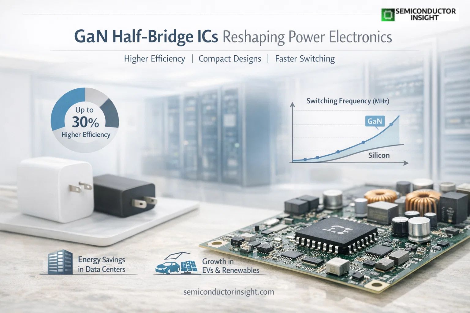
When built using GaN, these ICs operate at significantly higher switching frequencies compared to silicon-based MOSFETs. Typical GaN devices can switch in the range of several MHz, whereas traditional silicon solutions operate in lower kHz ranges. This shift reduces passive component size, making power systems smaller and lighter without compromising output.
To find out more, feel free to browse our latest updated report: https://semiconductorinsight.com/report/gan-half-bridge-ics-market/
Why GaN is becoming the material of choice?
- Gallium Nitride offers higher electron mobility and breakdown voltage, which translates into lower conduction and switching losses.
- In real-world deployments, GaN-based half-bridge ICs have demonstrated efficiency improvements of up to 30% in power conversion systems.
- Companies like Infineon and Texas Instruments have introduced integrated GaN solutions that reduce energy loss significantly in laptop chargers and telecom power supplies.
- The growing adoption of 65W to 240W fast chargers using GaN technology highlights how quickly the ecosystem is evolving.
- Where the real momentum is building?
- Consumer electronics is one of the strongest adoption zones. Fast charging adapters, gaming laptops, and compact power bricks are increasingly powered by GaN half-bridge ICs.
- A modern GaN charger can be nearly 40% smaller than its silicon counterpart while delivering the same output.
- Beyond consumer use, data centers are also emerging as a major application area.
- With global data center electricity consumption estimated at around 240 to 340 terawatt-hours annually, even small efficiency gains translate into massive energy savings.
- GaN-based power supplies are helping reduce heat generation and cooling requirements, directly impacting operational costs.
Design thinking is shifting rapidly
The integration of half-bridge GaN ICs is not just about replacing silicon components. It is influencing how engineers approach PCB design, thermal management, and EMI control. Higher switching speeds demand careful layout optimization to avoid noise and voltage spikes.
As a result, manufacturers are embedding protection features such as overcurrent protection, thermal shutdown, and dead-time control directly into ICs. This integration reduces external component count and simplifies system design for engineers working on compact devices.
Expanding footprint from electric mobility to scalable production
- GaN half-bridge ICs are steadily moving beyond consumer electronics into electric vehicles and renewable energy systems, where efficiency and compact design are critical.
- On-board chargers and DC-DC converters in EVs are increasingly adopting GaN configurations to reduce weight and energy loss, while solar inverters benefit from higher switching frequencies that enhance power density and responsiveness.
- At the same time, the broader GaN ecosystem is maturing rapidly, with foundries, packaging experts, and system integrators scaling up production capabilities.
- The transition from 6-inch to 8-inch wafers is improving yields and lowering costs, supported by strong industry collaborations and government-led semiconductor initiatives.
- This combined momentum in application expansion and manufacturing scale is making GaN half-bridge ICs more accessible and practical for widespread deployment.
A technology finding its rhythm in modern electronics
GaN Half-Bridge ICs Market is not driven by hype but by tangible engineering advantages. From compact consumer devices to energy-intensive infrastructure, the role of GaN is becoming more defined with each passing year. As engineers continue to push boundaries in power density and efficiency, GaN half-bridge ICs are emerging as a core building block in the evolving semiconductor landscape.

Comments (0)