
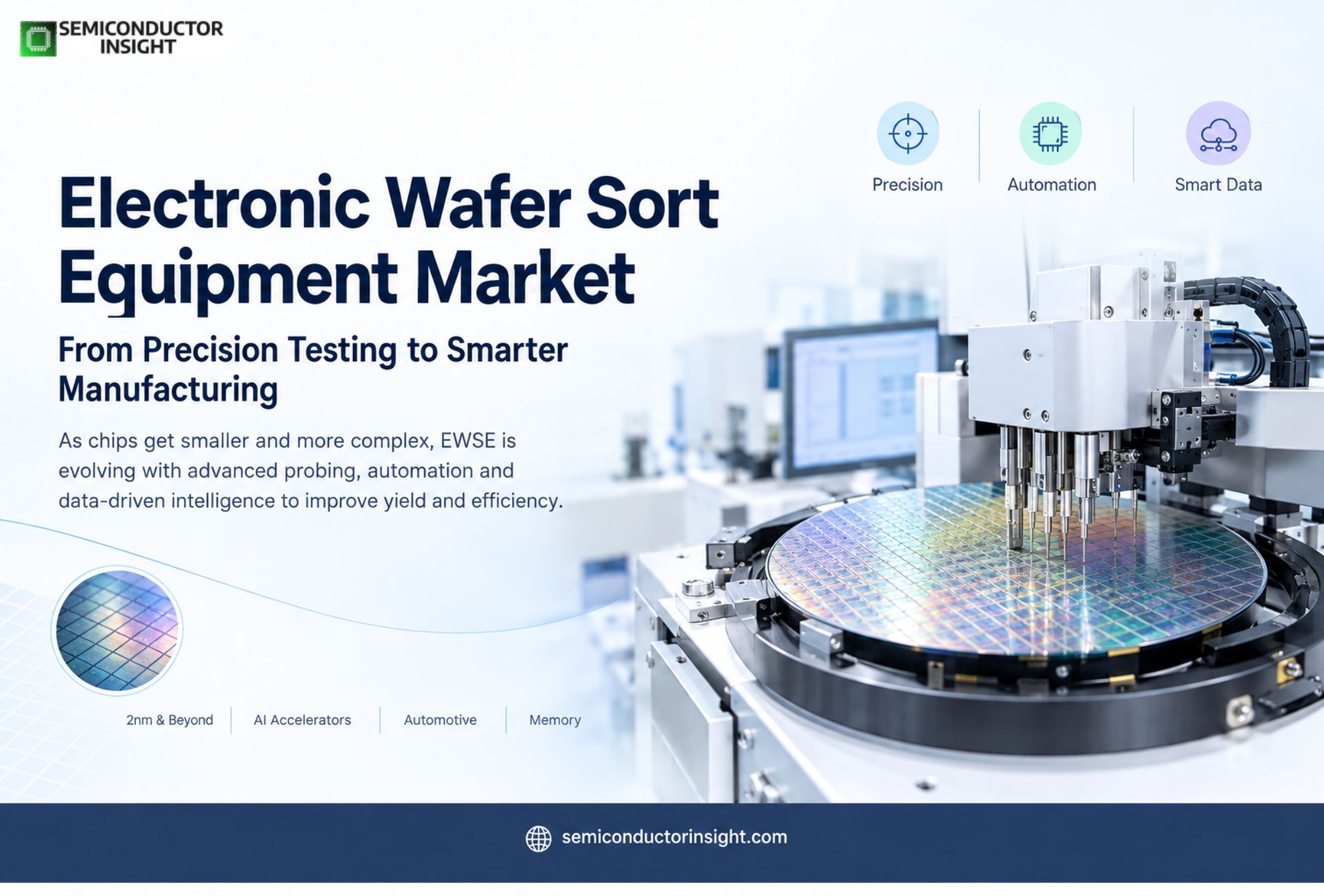
EWSE Market 2026: From 5nm to 2nm, Wafer Sort Technology Enters a New Phase
Semiconductor testing is no longer limited to a final quality check after fabrication. As chip architectures become denser and manufacturing costs rise, identifying defective dies while they are still on the wafer can prevent additional processing expenses and improve manufacturing efficiency. This is where Electronic Wafer Sort Equipment (EWSE) becomes important.
EWSE operates before wafer dicing and packaging, connecting semiconductor wafers with probing, measurement, classification, and automated handling processes. The growing complexity of AI processors, high-performance computing devices, automotive chips, memory products, and advanced logic is increasing the importance of accurate wafer-level electrical testing.
The 2nm Era Is Changing What “Precision” Means
- The semiconductor industry’s movement toward smaller process nodes is creating a more demanding environment for wafer sort operations. TSMC has announced advanced logic manufacturing plans involving 2nm technology, while other leading manufacturers are developing increasingly sophisticated process architectures.
- At these dimensions, tiny variations in electrical characteristics can influence device performance and yield. EWSE therefore needs to support tighter measurement tolerances, increasingly sophisticated probing technologies, faster test execution, and automated data handling.
- The transition from 3nm-class production toward 2nm-class manufacturing also means that wafer testing must generate increasingly useful information before individual dies move into packaging.
AI Accelerators Are Creating a Different Testing Profile
The rapid expansion of AI infrastructure is changing semiconductor test requirements. Modern AI accelerators can contain enormous numbers of transistors and are increasingly integrated with high-bandwidth memory and advanced packaging architectures.
This creates a testing environment where throughput matters alongside precision. A wafer containing thousands of dies can generate a substantial volume of test results, making automated classification and rapid data processing increasingly important.
- In 2025, global semiconductor sales reached approximately $791.7 billion, according to the Semiconductor Industry Association, highlighting the enormous scale of the semiconductor manufacturing ecosystem.
For EWSE suppliers, the significance is not simply the number of chips being produced. It is the increasing complexity of the devices being tested.
Probe Cards and Wafer Sorters Are Becoming More Connected
Modern wafer sort is increasingly dependent on the interaction between equipment, probe cards, handlers, software, and semiconductor test systems.
Probe technology has become particularly important as manufacturers test increasingly complex devices. High-density probing must maintain reliable electrical contact across repeated wafer movements while supporting increasingly demanding test conditions.
The equipment ecosystem is consequently becoming more integrated. Automated wafer alignment, optical inspection, probing, electrical measurement, defect classification, and manufacturing data systems increasingly work together rather than functioning as isolated stages.
Memory Testing Is Adding another Layer of Complexity
- Memory remains an important application environment for wafer-level testing. DRAM, NAND and emerging memory technologies require large-scale testing because even small defects can affect the economics of high-volume production.
- The rapid development of high-bandwidth memory for AI and data-center applications is particularly significant. HBM stacks multiple memory dies and relies on sophisticated packaging and interconnection technologies.
- Testing individual components before advanced assembly can help identify defective dies earlier in the manufacturing chain.
- This makes wafer-level test increasingly relevant to the broader AI hardware ecosystem rather than only traditional logic manufacturing.
Automotive Chips Are Raising the Reliability Bar
Automotive semiconductors introduce another dimension to wafer testing because devices used in vehicles must operate reliably across demanding temperature, electrical, and environmental conditions.
The shift toward electric vehicles, advanced driver-assistance systems, battery-management electronics, and software-defined vehicles is increasing semiconductor content per vehicle. The International Energy Agency reported that global electric car sales exceeded 17 million units in 2024, demonstrating the scale of electrification-related semiconductor demand.
For EWSE, this translates into stronger attention to parametric testing, defect screening, traceability, and reliable classification before devices proceed to packaging.
For a more thorough report, please contact us using our most recent report:
https://semiconductorinsight.com/report/ewse-market/
Data Is Becoming Part of the Equipment
One of the most important changes around wafer sort is the growing value of test data. Each wafer can produce extensive electrical measurements that reveal patterns associated with process variation, defects, or device performance.
Manufacturers can use this information to connect wafer-level results with fabrication processes and yield-management systems. Equipment capable of collecting, organizing, and transferring this information efficiently can therefore contribute beyond the physical act of sorting dies.
This shift is moving EWSE toward a more data-intensive role inside semiconductor fabs.
What 2026 Means for the EWSE Equipment Stack?
The EWSE landscape is evolving alongside the semiconductor industry’s transition toward 2nm-class logic, AI accelerators, HBM, advanced packaging, automotive electronics, and increasingly automated fabs.
The next generation of wafer sort equipment is consequently being shaped by three practical requirements: precision at smaller geometries, higher throughput for increasingly expensive wafers, and deeper integration with manufacturing data.
As semiconductor manufacturers invest in new fabrication capacity across the United States, Taiwan, South Korea, Japan, Europe, and other production hubs, wafer-level testing is becoming an increasingly important link between fabrication output and packaged-chip quality. The result is a changing EWSE ecosystem where equipment performance increasingly depends on how effectively hardware, probing, automation, measurement, and data systems operate together.

Comments (0)