

EUV vs. DUV Technologies in the Semiconductor Lithography Equipment Market Which Leads Advanced Chip Production
The global semiconductor lithography equipment market size is estimated at approximately USD 29 billion in 2026, supported by accelerating investments in advanced semiconductor fabrication facilities, artificial intelligence processors, high-performance computing, automotive electronics, and next-generation memory manufacturing.
The market continues to benefit from the industry’s migration toward 3 nm and 2 nm process technologies, where advanced lithography systems remain the foundation of transistor scaling and production efficiency. Increasing capital expenditure from major foundries and integrated device manufacturers is expected to sustain equipment demand through the remainder of the decade.
Why Every Advanced Chip Starts with Lithography?
Every smartphone processor, AI accelerator, automotive controller, and memory chip begins with one critical manufacturing step lithography. This process transfers microscopic circuit patterns from photomasks onto silicon wafers using highly specialized optical systems and photoresists. As transistor dimensions continue shrinking, manufacturers require increasingly sophisticated lithography equipment capable of producing features measured in only a few nanometers.
The surge in AI infrastructure has dramatically increased demand for advanced logic chips, pushing semiconductor manufacturers to expand fabrication capacity. This expansion directly translates into greater demand for precision lithography systems capable of supporting higher wafer throughput while maintaining atomic-scale accuracy.
The New Manufacturing Race Is Happening Inside Semiconductor Fabs
• Rather than competing solely on chip design, leading semiconductor companies are now competing on manufacturing capability. Governments and private investors worldwide are funding fabrication projects to strengthen domestic semiconductor production.
• Global semiconductor sales surpassed USD 627 billion in 2024, according to the Semiconductor Industry Association, underscoring the expanding demand for cutting-edge manufacturing equipment throughout the supply chain.
• Meanwhile, the World Semiconductor Trade Statistics (WSTS) projects continued industry expansion supported by AI computing, automotive electronics, and cloud infrastructure.
• These production trends are creating sustained demand for lithography equipment capable of supporting increasingly complex device architectures.
Precision at the Atomic Scale
Modern lithography has evolved far beyond conventional optical imaging. Today’s leading systems integrate advanced optics, precision stages, laser-produced plasma light sources, computational imaging, and sophisticated metrology into a single manufacturing platform.
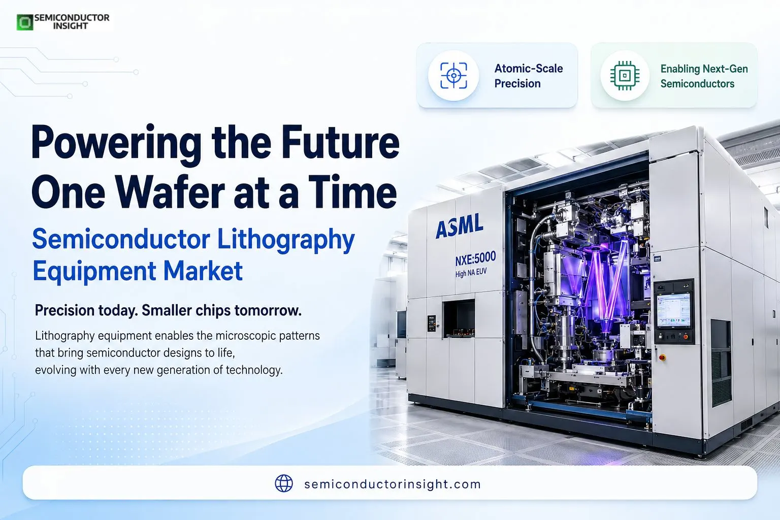
A notable milestone arrived with the commercialization of High Numerical Aperture Extreme Ultraviolet (High NA EUV) lithography, enabling manufacturers to improve pattern resolution for future technology nodes while reducing multiple patterning steps. This advancement improves manufacturing efficiency while supporting continued transistor miniaturization.
Industry estimates indicate that a single advanced EUV lithography platform may contain over 100,000 individual components, weigh more than 180 metric tons, and require several cargo aircraft and specialized logistics teams for global delivery and installation.
For a more thorough report, please contact us using our most recent report: https://semiconductorinsight.com/report/semiconductor-lithography-systems-refurbishment-market/
AI Is Quietly Reshaping Equipment Requirements
ü Artificial intelligence is influencing semiconductor manufacturing long before chips reach data centers. Machine learning algorithms are increasingly used inside lithography equipment for predictive maintenance, overlay optimization, defect detection, and process control.
ü Manufacturers are also deploying digital twins that simulate lithography processes before production begins, reducing engineering cycles and improving wafer yield. Combined with advanced computational lithography software, these technologies allow fabs to maximize productivity while minimizing material waste and equipment downtime.
ü The result is a manufacturing environment where software intelligence has become nearly as important as optical precision.
Recent Industry Developments worth Watching
Several developments continue to redefine the global lithography landscape.
Large-scale semiconductor manufacturing investments announced across the United States, Europe, Japan, South Korea, and Taiwan are increasing long-term equipment procurement. Government initiatives supporting domestic chip manufacturing have accelerated construction of new fabrication facilities dedicated to advanced logic and memory production.
Leading foundries are also expanding production for AI accelerators, advanced packaging, and high-bandwidth memory, all of which require increasingly sophisticated lithographic processes. Simultaneously, research organizations are exploring next-generation patterning methods that may complement optical lithography for specialized semiconductor applications over the coming decade.
Beyond Smaller Chips
• Lithography is no longer focused only on reducing transistor dimensions. Modern equipment supports innovations across diverse semiconductor applications including advanced packaging, chiplet integration, silicon photonics, MEMS sensors, image sensors, radio frequency devices, and power semiconductors.
• For electric vehicles, highly reliable semiconductor devices require precise manufacturing processes that begin with accurate wafer patterning. Similarly, optical communication chips supporting AI data centers depend on advanced lithography to achieve greater integration density and lower power consumption.
• This broadening application landscape ensures that lithography equipment remains relevant far beyond traditional CPU manufacturing.
Innovation Indicators That Deserve Attention
Several measurable indicators demonstrate the accelerating pace of lithography innovation.
Global semiconductor manufacturers continue investing tens of billions of dollars annually in fabrication expansion. Advanced logic production increasingly targets 2 nm technology nodes, while pilot development programs have already begun exploring future generations below this threshold.
Research organizations are simultaneously improving photoresist materials, mask inspection technologies, computational lithography software, and precision metrology systems to enhance manufacturing accuracy without sacrificing throughput. These parallel innovations collectively strengthen the long-term outlook for semiconductor lithography equipment.

Comments (0)