

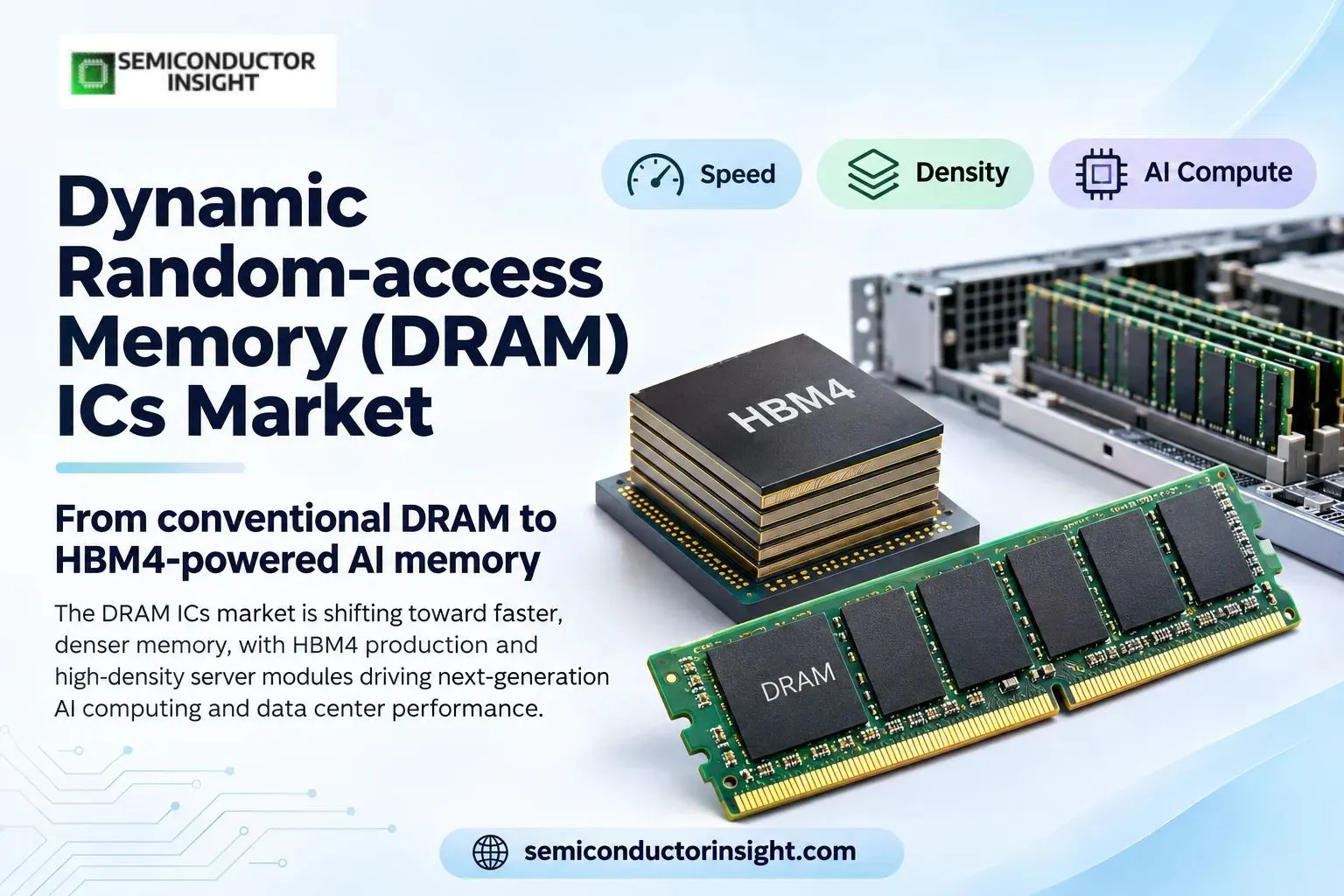
Dynamic Random-access Memory (DRAM) ICs Market in 2026 as HBM4 Production and High-Density Server Memory Redefine Semiconductor Manufacturing
The performance of modern semiconductor systems is no longer determined exclusively by processor speed. Artificial intelligence, high-performance computing and large-scale data processing are placing greater importance on how quickly processors can access and exchange information. This shift is bringing Dynamic Random-access Memory (DRAM) ICs into a more strategic position within semiconductor manufacturing.
DRAM stores data temporarily in memory cells consisting of a transistor and capacitor, allowing processors to retrieve information during active computing operations. Its applications range from smartphones and laptops to automotive electronics, cloud servers, graphics processors and industrial computing systems. However, the increasing complexity of AI workloads is changing traditional requirements for memory density, bandwidth and energy efficiency.
HBM4 Is Changing How Memory Chips Are Designed for AI Accelerators
- High-Bandwidth Memory is becoming one of the most important technology developments in advanced DRAM manufacturing. Instead of relying on conventional memory modules positioned separately from processors, HBM stacks multiple DRAM dies vertically and connects them through through-silicon vias (TSVs).
- In February 2026, Samsung announced commercial HBM4 production, featuring a 2,048-bit interface, 11.7 Gbps operating speed and the ability to reach 13 Gbps. The technology uses a 4 nm logic base die alongside sixth-generation 10 nm-class DRAM processing.
- Micron also entered high-volume HBM4 production in March 2026 with its 36 GB 12-high product, delivering bandwidth above 2.8 TB/s. The company additionally sampled 48 GB 16-high products for customers. These developments demonstrate how memory manufacturers are increasingly competing through stack height, bandwidth and integration rather than conventional chip density alone.
DDR5 MRDIMMs Are Addressing the Memory Bottleneck in Server Platforms
While HBM receives considerable attention in AI accelerator development, conventional DRAM remains essential for server processors and general-purpose computing.
Multiplexed Rank DIMMs (MRDIMMs) are emerging as an important development in the DDR5 ecosystem. By using multiplexed data-buffer technology, these modules allow multiple memory ranks to operate in parallel, improving effective data-transfer performance.
The JEDEC-standardized DDR5 ecosystem received an important update in 2026 with the JESD82-552 Gen2 multiplexed-rank data-buffer specification. This development supports next-generation memory modules targeting data rates of up to 12,800 MT/s, making them relevant to increasingly demanding server workloads.
You Can Go Through Our Latest Updated Insights Here: https://semiconductorinsight.com/report/dynamic-random-access-memory-dram-ics-market/
Semiconductor Manufacturing Is Moving Toward More Advanced DRAM Nodes
- Manufacturing efficiency is becoming increasingly important as DRAM manufacturers attempt to increase the number of memory bits produced from each wafer. Advanced lithography, process integration, capacitor scaling and improved transistor structures are central to this transition.
- Samsung’s HBM4 production uses its 1c DRAM process, while Micron’s advanced HBM roadmap incorporates its 1-beta and upcoming 1-gamma process technologies.
- Micron’s manufacturing expansion also illustrates the scale of infrastructure required. Its first Idaho DRAM fabrication facility is expected to begin wafer output in mid-2027, while its second Idaho facility targets initial output in late 2028.
- The company’s first New York fabrication facility is expected to begin production in 2030. These projects demonstrate how AI-related memory requirements are influencing long-term semiconductor manufacturing investments.
The 48 GB Memory Stack Is Raising Expectations for AI Computing
At CES 2026, SK hynix showcased a 16-layer HBM4 product with 48 GB capacity, following its 12-layer 36 GB HBM4 design. The company also presented SOCAMM2 and LPDDR6 technologies, highlighting the increasing importance of memory solutions tailored to different computing environments.
The additional six layers compared with an eight-layer configuration and the transition from 36 GB to 48 GB illustrate how manufacturers are increasing capacity within individual memory packages. Higher-capacity stacks can support larger AI models and more demanding data-intensive operations, although thermal management and packaging complexity remain important engineering considerations.
Memory Is Becoming a System-Level Design Decision
The next stage of DRAM development will depend on coordination between memory manufacturers, processor designers, packaging companies and semiconductor foundries. HBM4E, CXL-enabled memory expansion, advanced DDR5 modules and low-power mobile DRAM are creating different solutions for different computing requirements.
SK hynix highlighted this direction at Future of Memory and Storage 2026, demonstrating CXL-based pooled memory and tiered memory architectures for AI workloads. Such developments indicate that DRAM innovation is moving beyond individual chip performance toward complete computing-system optimization.

Comments (0)