Disco’s Next-Gen SiC Blades and K&S Distribution Expansion Propel Dicing Blades Market Toward $446.7 Million by 2032
In the ever-evolving world of semiconductor technology, precision and miniaturization are everything. As chips grow smaller and more complex, every micron matters. At the heart of this intricate dance lies a critical, often overlooked component — the dicing blade. These ultra-thin, high-performance blades are responsible for slicing silicon wafers into individual dies without damaging their delicate structures.
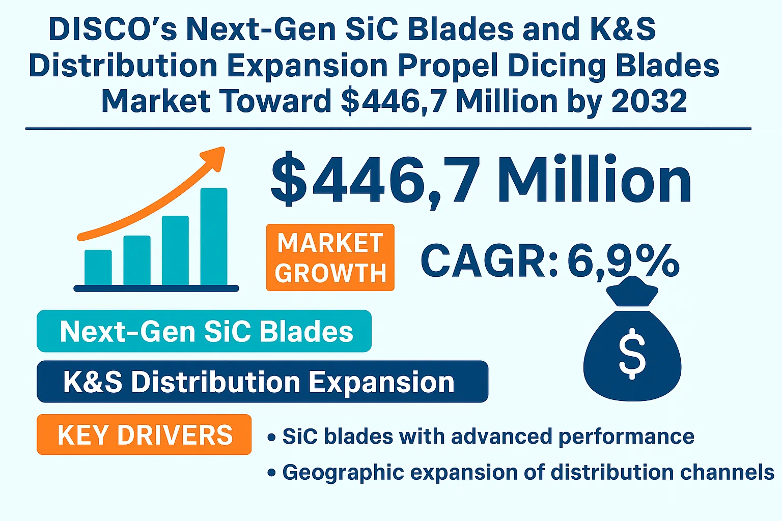
The global Dicing Blades for Semiconductor Packaging Market is currently undergoing a dynamic transformation. Valued at US$ 267.3 million in 2024, the market is projected to soar to US$ 446.7 million by 2032, growing at a CAGR of 6.7% during the forecast period of 2025 to 2032. This growth is being driven by significant technological innovations, increased demand for compound semiconductors, and the industry’s shift toward advanced packaging solutions.
Access Your Free Sample Report- Dicing Blades for Semiconductor Packaging Market
The Role of Dicing Blades in Semiconductor Packaging
Dicing blades are precision tools designed to cut through semiconductor wafers to separate individual dies, or “chips.” They come in various types, including:
- Resin bond blades
- Metal bond blades
- Electroformed nickel blades
- Hubbed and hubless variants
Their usage varies depending on the substrate material (silicon, SiC, GaN), wafer thickness, and cutting method (mechanical sawing vs. laser dicing). In semiconductor packaging — particularly fan-out wafer-level packaging (FOWLP) and 3D ICs — clean, damage-free singulation is critical.
Market Drivers
- Miniaturization and Advanced Packaging
As chipmakers transition to 3nm and smaller nodes, wafer-level packaging becomes more prevalent. Dicing blades must now deliver ultra-thin, low-kerf cutting with minimal chipping — especially for high-density packages used in AI chips, smartphones, and automotive ECUs.
- Rising Demand for SiC and GaN Devices
With power electronics booming in electric vehicles and 5G, materials like silicon carbide (SiC) and gallium nitride (GaN) are gaining traction. These hard, brittle materials require superabrasive blades with optimized diamond grit and bond formulations.
- Global Semiconductor Supply Chain Expansion
Regions such as India, Vietnam, Eastern Europe, and Mexico are witnessing rising investment in local semiconductor fabs and packaging facilities. This geographical expansion fuels demand for dicing solutions compatible with diverse wafer types.
Recent Industry Developments
Let’s explore some of the most notable innovations and strategic moves by leading companies shaping this space:
Disco Corporation’s Dual Blade Launch (2024)
In late 2024, Disco Corporation, a leading Japanese manufacturer of dicing and grinding equipment, introduced two new dicing blade series:
- ZHSC25 Series: Engineered specifically for silicon carbide (SiC) wafers. These blades are equipped with high-density diamond grits and advanced bond technology, allowing for deeper cuts with minimal vibration and micro-cracking.
- Z25 Series: Optimized for electronic components like MLCCs and power transistors. These blades offer excellent wear resistance and are compatible with ultra-thin die structures.
This dual launch positions Disco to capture growth in both traditional silicon and emerging wide-bandgap semiconductor markets.
Inseto Expands Distribution of K&S Dicing Blades in Europe
In May 2024, Inseto, a prominent UK-based distributor, became the exclusive European supplier for Kulicke & Soffa’s (K&S) hubbed dicing blades across Austria, Germany, the Netherlands, and Portugal.
K&S’s blades are known for their:
- Customizable diamond concentration and binder types
- Low-damage profiles for delicate dies
- Compatibility with high-speed dicing systems
This strategic move enhances access to premium blade technologies in Europe — especially important as EU fabs ramp up production under the European Chips Act.
Download Sample Report PDF- Dicing Blades for Semiconductor Packaging Market
Technology Trends Reshaping the Dicing Blade Industry
- Smart Manufacturing and Predictive Maintenance
The rise of Industry 4.0 has introduced smart blades embedded with micro-sensors. These can track wear rate, temperature, vibration, and cutting resistance in real-time. Data analytics and machine learning help operators:
- Optimize blade change intervals
- Predict potential blade failures
- Improve overall tool performance
This not only extends blade life but also boosts yield and throughput.
- Laser Dicing Integration
Though traditional blade-based dicing remains dominant, hybrid systems that combine mechanical dicing with stealth laser dicing (SLD) are gaining popularity — especially in cutting fragile wafers like image sensors and MEMS. Dicing blades used in tandem with lasers must be optimized for post-laser die singulation processes.
- Environmental Sustainability
Blade manufacturers are now incorporating eco-friendly practices, including:
- Use of recycled metals and bio-based resins in bond formulations
- Reduced water usage and kerf loss during wafer slicing
- Packaging made from biodegradable materials
These steps align with broader ESG goals adopted across the semiconductor ecosystem.
Challenges in the Market
- Brittle Substrate Complexity
SiC and GaN materials fracture unpredictably. Dicing them without edge chipping requires blade customization and real-time force modulation, raising R&D and production costs.
- Tooling Costs and Maintenance
Dicing blades require high-precision fabrication and frequent replacement. Tooling downtime for blade changeover can be costly, especially for high-volume fabs.
- Regional Supply Chain Gaps
Not all semiconductor regions have easy access to advanced blades. For example, many Southeast Asian back-end facilities still rely on imported tooling, which adds cost and logistical delays.
Market Segmentation Overview
By Blade Type
- Resin bond blades (ideal for thin wafers, flexible electronics)
- Metal bond blades (used for hard substrates like SiC)
- Electroformed nickel blades (used in optical and MEMS devices)
By Wafer Material
- Silicon
- Silicon carbide (SiC)
- Gallium nitride (GaN)
- Sapphire
- Glass
By End Use
- Consumer electronics (smartphones, wearables)
- Automotive (ADAS, EV control units)
- Industrial electronics (power modules, MEMS)
- Data centers (AI, high-performance computing)
Regional Market Insights
Asia-Pacific — Dominant and Growing
With countries like Taiwan, South Korea, China, and Japan housing major chipmakers and packaging houses, APAC dominates the dicing blade market. Disco Corporation, Tokyo Seimitsu, and South Korea’s EO Technics are key regional players.
🇺🇸 North America — R&D Powerhouse
Home to Intel, Texas Instruments, and GlobalFoundries, the U.S. focuses on advanced packaging R&D, fueling demand for ultra-thin and hybrid dicing technologies.
🇪🇺 Europe — Strategic Expansion
Driven by the EU Chips Act, new packaging facilities across Germany, France, and the Netherlands are increasing imports of high-precision dicing tools. Partnerships like Inseto and K&S further bolster the ecosystem.
Competitive Landscape
| Company | Key Strengths |
| Disco Corp. | Leader in dicing saws and blades; strong in APAC |
| Kulicke & Soffa | Known for hubbed blades and global supply chain |
| Tokyo Seimitsu | High-precision cutting tools; focus on automation |
| Advanced Dicing Technologies (ADT) | Strong in hybrid dicing solutions |
| UKAM Industrial | Custom blade engineering for niche markets |
Startups and niche players are emerging in the precision blade design space, offering customized solutions for AI, biomedical chips, and flexible electronics.
Click Here To Download Full Sample Report- Dicing Blades for Semiconductor Packaging Market
Future Outlook (2025–2032)
The dicing blade market is set to witness substantial shifts over the next decade:
- Wider Adoption of AI Chips and 3D ICs will require next-gen blades with higher accuracy and minimal chipping.
- Automation and Robotics will reduce reliance on human skill in blade setup and changeover.
- Localized Supply Chains will encourage regional blade manufacturing in India, Eastern Europe, and LATAM.
- Digital Twins of dicing blades — virtual simulations to predict blade behavior — may become standard in fab environments.
As we move further into the age of edge computing, quantum processors, and smart sensors, the humble dicing blade will continue playing a silent but critical role.
From wafer to world-changing device, every chip’s journey begins with a slice — a cut made with extraordinary precision. Dicing blades, though often overlooked, are indispensable in this transformation. As the global Dicing Blades for Semiconductor Packaging market grows from US$ 267.3 million in 2024 to US$ 446.7 million by 2032, the industry is not only scaling up but also evolving in intelligence, sustainability, and global reach.
The future belongs to those who can cut cleanly, efficiently, and smartly. And in the fast-paced world of semiconductors, the right blade makes all the difference.
Comments (0)