
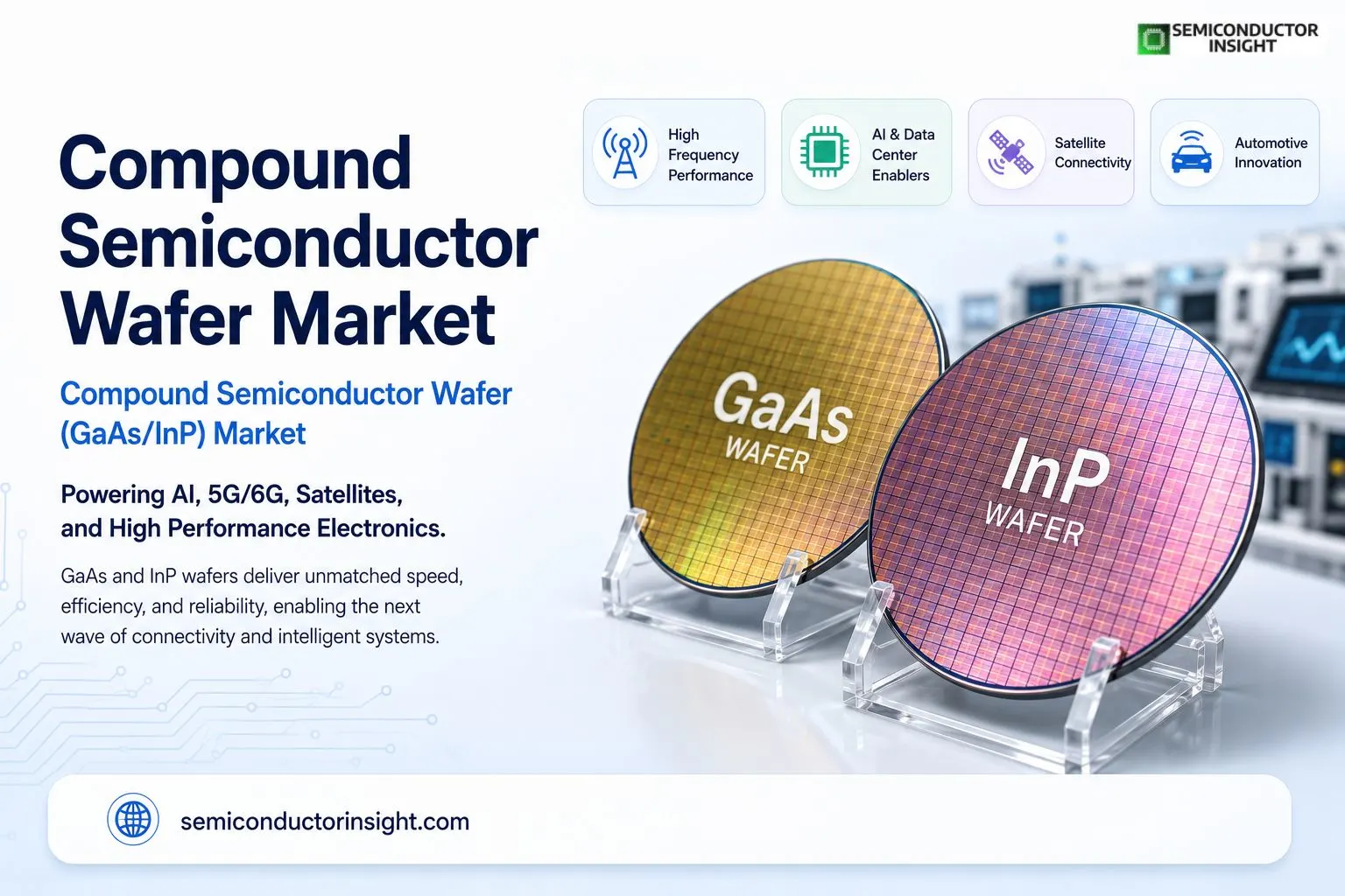
Compound Semiconductor Wafer Market Reshaping High Frequency Electronics and AI Hardware Demand
The semiconductor industry is no longer powered only by silicon. A growing layer of high-performance electronics now depends on compound semiconductor wafers such as gallium arsenide (GaAs) and indium phosphide (InP), materials that are rapidly moving from niche applications into mainstream infrastructure. From AI networking and satellite internet systems to automotive radar and high-speed optical communication, these wafers are becoming foundational to the future digital economy.
Unlike conventional silicon substrates, compound semiconductors offer faster electron mobility, higher frequency performance, and lower signal loss. This is why telecom giants, defense manufacturers, and hyperscale data center operators are increasing investments in GaAs and InP technologies as global data traffic intensifies.
AI Servers Are Quietly Expanding the Need for InP Wafers
- Artificial intelligence has dramatically increased pressure on data center bandwidth. AI clusters require ultra-fast optical communication between GPUs, switches, and storage systems. This is where indium phosphide wafers are gaining global relevance.
- InP-based photonic integrated circuits are increasingly used in coherent optical transceivers supporting 400G, 800G, and emerging 1.6T optical networking.
- According to data from the International Telecommunication Union (ITU), global internet traffic surpassed 1 zettabyte annually in recent years, accelerating the need for advanced optical transmission systems. Telecom operators in the United States, Japan, and South Korea are expanding fiber backbone networks that rely heavily on InP laser technologies.
- Major cloud infrastructure providers are also investing in optical interconnect startups focused on indium phosphide integration. Startups working on co-packaged optics are exploring InP-based laser modules to reduce power consumption and latency inside AI data centers.
GaAs Chips Continue Dominating Smartphone RF Architectures
While AI infrastructure is creating opportunities for InP wafers, GaAs wafers continue to dominate radio frequency applications. Modern smartphones contain multiple GaAs power amplifiers that enable stable 5G connectivity across different spectrum bands.
The expansion of 5G Advanced and early-stage 6G research is increasing the complexity of RF front-end modules. This shift benefits gallium arsenide because of its ability to handle high-frequency signals with superior efficiency compared to traditional silicon alternatives.
According to data published by the GSM Association, global 5G connections are expected to cross billions of users before the end of the decade, creating sustained demand for RF semiconductor components. Companies supplying GaAs epitaxial wafers are therefore scaling production capacities, particularly in Taiwan, Japan, and the United States.
The automotive sector is also contributing to GaAs demand. Advanced driver assistance systems and automotive radar increasingly require compound semiconductor materials for high-frequency sensing capabilities used in autonomous driving platforms.
Stay connected for additional in-depth information right here: https://semiconductorinsight.com/report/compound-semiconductor-wafer-gaas-inp-market/
Satellite Internet Projects Are Creating a Fresh Demand Wave
- Low Earth orbit satellite projects are changing the demand profile for compound semiconductor wafers. Satellite communication systems require highly reliable RF chips and optical communication devices capable of operating under extreme environmental conditions.
- GaAs solar cells are already widely used in satellites because of their radiation resistance and high conversion efficiency. At the same time, InP technologies are being explored for laser-based inter-satellite communication systems designed to improve data transmission speeds in space networks.
- Recent launches from private aerospace firms and government-backed satellite programs have intensified research partnerships between semiconductor fabs and aerospace contractors. Europe, the United States, and China are actively funding satellite communication infrastructure to reduce dependency on terrestrial broadband systems.
Semiconductor Manufacturing Strategies Are Expanding Beyond Silicon
Governments worldwide are supporting semiconductor diversification strategies after recent supply chain disruptions exposed vulnerabilities in global chip production.
Japan has increased support for advanced material research through collaborations involving universities and semiconductor companies focused on next-generation wafers. The United States CHIPS and Science Act has also accelerated investment discussions around specialty semiconductor manufacturing, including compound semiconductor facilities.
Several wafer manufacturers are adopting larger wafer diameters to improve production economics. While 4-inch and 6-inch wafers remain standard for many applications, research around 8-inch compound semiconductor wafer production is gaining traction to support higher manufacturing volumes.
This manufacturing transition is important because compound semiconductor fabrication remains more expensive and technically demanding than silicon production. Improvements in substrate quality, defect reduction, and epitaxial growth processes are becoming critical competitive factors.
Defense Electronics Push Material Innovation Further
Modern defense systems increasingly depend on compound semiconductor wafers for radar, electronic warfare, secure communication, and infrared sensing technologies.
GaAs-based monolithic microwave integrated circuits are widely used in phased-array radar systems because they support high-frequency operation and thermal stability. Meanwhile, indium phosphide components are being integrated into ultra-sensitive photodetectors used in secure optical communication networks.
Global defense modernization programs are accelerating procurement of advanced sensing platforms, indirectly strengthening long-term demand for specialty semiconductor wafers.
Key Market Data Points
- According to the International Energy Agency, global data center electricity consumption is expected to continue rising sharply due to AI workloads and cloud expansion.
- The GSM Association estimates billions of active 5G connections globally before 2030, increasing RF semiconductor demand.
- NASA and multiple aerospace agencies continue using GaAs solar technologies in satellite systems because of higher radiation tolerance.
- The United States CHIPS and Science Act includes over USD 50 billion in semiconductor manufacturing and research incentives.
- Japan, South Korea, Taiwan, and the United States remain major hubs for compound semiconductor wafer production and epitaxial processing.
Universities and Research Labs Are Building the Next Breakthroughs
In order to combine performance and cost-effectiveness, research institutions are increasingly concentrating on combining compound semiconductors with silicon photonics. Future processors may be able to directly integrate InP optical communication and silicon logic on advanced packaging due to hybrid integration techniques.
Scientists are also experimenting with terahertz communication systems, an area expected to influence future 6G infrastructure development. Compound semiconductor wafers are viewed as essential materials for these ultra-high-frequency applications.
In Europe, collaborative semiconductor research projects are exploring energy-efficient photonic computing systems that could reduce data center electricity consumption significantly over the coming decade.

Comments (0)