

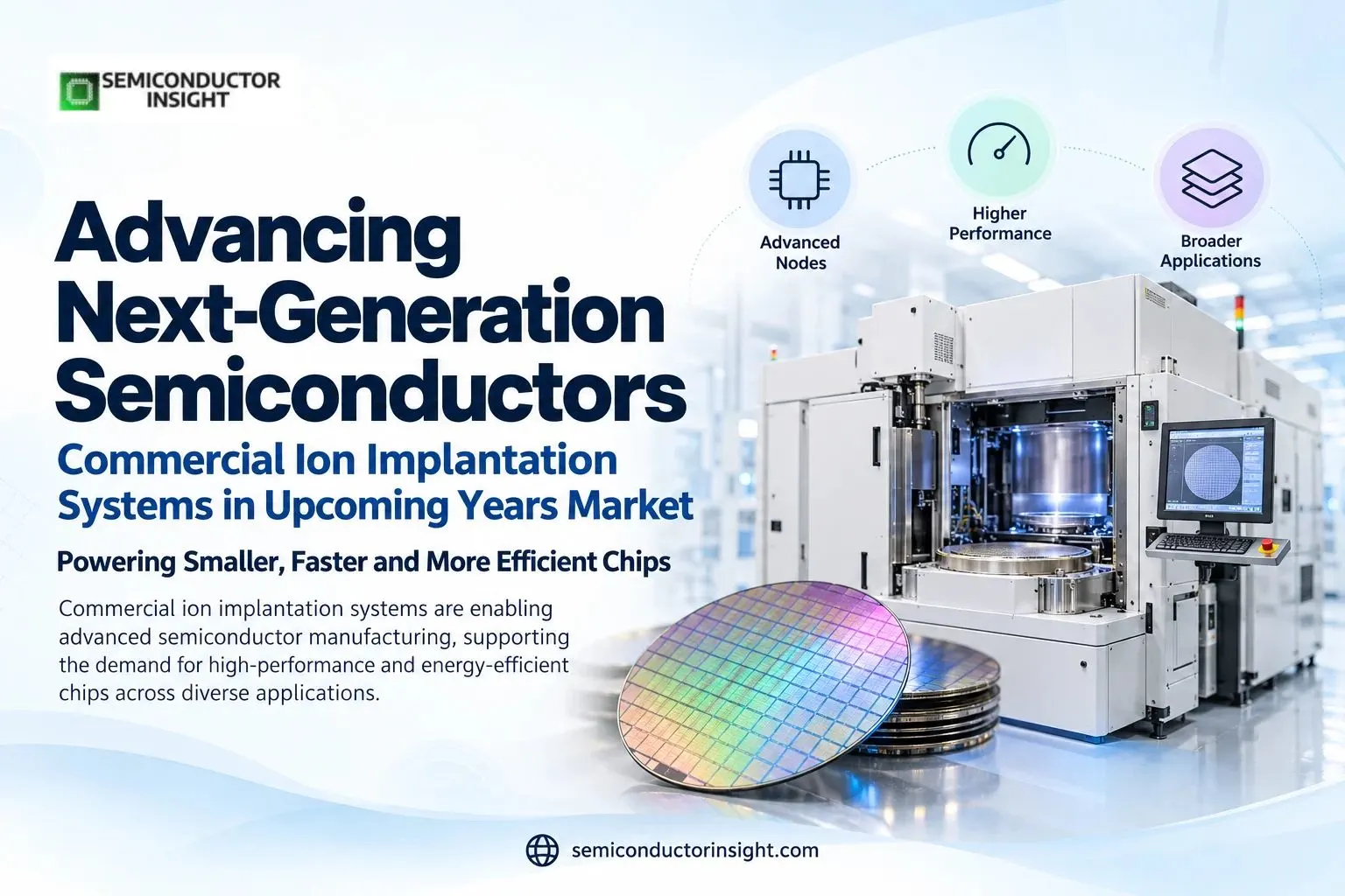
Commercial Ion Implantation Systems in Upcoming Years Market Fuels High-Current Platforms, Advanced Doping and Fab Productivity
Ion implantation is one of the less visible stages of semiconductor manufacturing, but it directly determines where and how electrical characteristics are created in a wafer. During implantation, ions are introduced into selected areas of semiconductor material to alter its electrical properties. Samsung describes phosphorus and arsenic as examples of Group 15 dopants used for n-type material, while Group 13 elements such as boron support p-type characteristics. Samsung Semiconductor Global
ASML notes that ion implantation can be repeated within the broader sequence of semiconductor processing, while modern chip fabrication can involve as many as 100 patterned layers.
2026 Opens with a New High-Current Implanter
- One of the year’s clearest equipment signals came from Axcelis in February 2026 with the introduction of the Purion H6. The company positioned the system for high-current applications spanning logic, advanced memory, image sensors and mature semiconductor technologies.
- The system combines a high-throughput beamline with new dose-control, particle-control and ion-source technologies. Axcelis says its design is intended to improve beam stability, repeatability and productivity while reducing maintenance requirements.
- This development shows how the commercial equipment market is shifting from simply delivering an ion beam toward controlling the entire implant process with greater consistency.
A 15 MeV Qualification Highlights the High-Energy Opportunity
High-energy implantation is gaining renewed attention as device architectures become more specialized. In July 2026, Axcelis announced that its Purion XEmax completed an evaluation at a leading semiconductor foundry for an emerging power-management integrated-circuit application requiring implantation capability up to 15 MeV.
The number is significant from an equipment perspective because it demonstrates how commercial systems are being designed around substantially different energy windows rather than a single mainstream implant regime.
SiC Is Creating a Different Equipment Playbook
The strongest specialized opportunity is coming from wide-bandgap power devices. At the 2026 International Conference on Ion Implantation and Annealing Technology, Axcelis highlighted work involving SiC superjunction MOSFETs, aluminum implantation, channeling effects, within-wafer implant uniformity and co-optimization of implantation and annealing.
The company also presented SiC-related work at SEMICON China 2026, including implantation approaches for reducing the cost of SiC superjunction structures.
That matters because SiC does not simply replicate silicon processing. Implant energy, dopant activation, crystal effects and annealing behavior create different equipment requirements.
Throughput Is Being Measured in Wafers, Not Just Beam Power
Commercial implanters are increasingly differentiated by the combination of beam capability and wafer-handling productivity. Axcelis reports throughput of up to 500 wafers per hour for its Purion platform, while its product family spans high-current, medium-current, medium-energy and high-energy configurations.
A useful way to view the equipment stack is:
Ion source → beam generation → mass/energy control → wafer positioning → dose measurement → process verification → annealing
The commercial opportunity therefore extends beyond the primary implantation chamber into beam monitoring, metrology, automation and process-control technologies.
To find out more, feel free to browse our latest updated report: https://semiconductorinsight.com/report/global-commercial-ion-implantation-systems-market/
Korea Becomes a Manufacturing Expansion Point
In September 2026, Axcelis announced a planned $35 million investment to build a new ion-implantation equipment manufacturing facility in Pyeongtaek, South Korea. The planned site covers approximately 200,000 square feet and is expected to include warehousing, Class 1,000 and Class 10,000 clean rooms and a training center. A groundbreaking ceremony is scheduled for October 20, 2026.
The announcement is notable because it connects equipment demand with local manufacturing infrastructure rather than treating semiconductor capital equipment as a purely export-oriented business.
The Equipment Map Is Becoming More Diverse
- The 2026 SEMICON ecosystem illustrates the breadth of implantation technology.
- Sumitomo Heavy Industries Material Solutions lists medium-current, high-current and high-energy systems, with published energy ranges extending from 0.2 keV to 14,400 keV depending on platform.
- Its high-energy equipment is positioned for applications including image sensors, while its systems also address power-device processing. Expo
- That range reinforces a central characteristic of the Commercial Ion Implantation Systems Market: there is no single “standard” implanter for every fab.
What Fab Expansion Means for Ion Implant Equipment?
The current market is increasingly tied to the diversification of semiconductor manufacturing itself. Advanced logic and memory demand precision and repeatability, image sensors require high-energy implantation capabilities, while power semiconductors are creating new requirements around SiC and other wide-bandgap materials.
With new equipment platforms, specialized SiC process development and additional manufacturing capacity emerging during 2026, commercial ion implantation is moving from a mature back-end-of-the-process tool category into a more strategically visible part of fab technology planning.

Comments (0)