
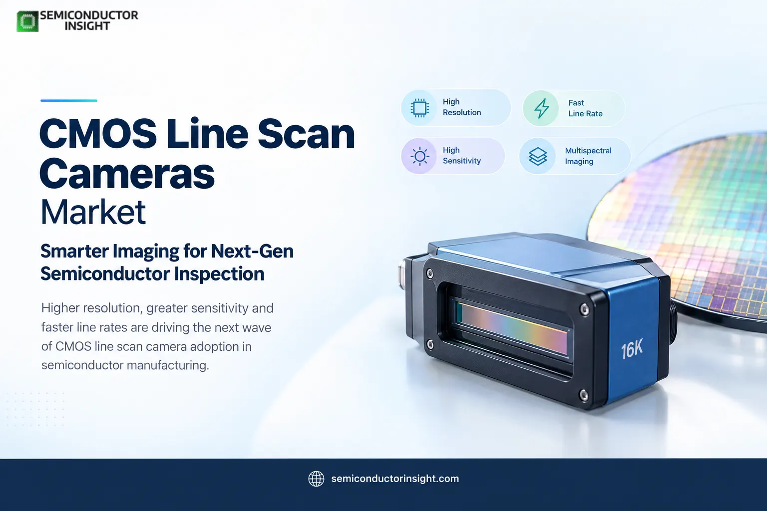
CMOS Line Scan Camera Market 2026: 16K Resolution and 1 MHz Scanning Redefine High-Speed Inspection
Semiconductor manufacturing increasingly depends on imaging systems that can detect extremely small defects without slowing production equipment. CMOS line scan cameras are particularly suited to this environment because they capture one line of an object at a time while the wafer, panel or material moves through the inspection field. Instead of taking conventional two-dimensional frames, the system builds an image continuously from successive lines.
That architecture makes line scan imaging attractive for wafer inspection, packaging, PCB inspection and other processes where motion is continuous. Basler notes that TDI line scan cameras are already used extensively for semiconductor and electronics inspection because they combine high sensitivity with fast acquisition.
Why semiconductor surfaces are becoming harder to image?
- Inspection conditions are becoming increasingly demanding. Semiconductor surfaces can contain reflective structures, extremely small pattern variations and defects that are difficult to distinguish under limited illumination.
- Teledyne DALSA points out that feature sizes in semiconductor wafer inspection have decreased by a factor of 3.3 in each dimension, equivalent to approximately 10.8 times greater demand across two dimensions, while wafer size increased from 200 mm to 300 mm.
- The company estimates that the combined speed and resolution requirement has increased by roughly 25 times.
- This combination explains why simply increasing camera resolution is not enough. Inspection systems need speed, sensitivity, low noise and stable image acquisition at the same time.
16K imaging changes the performance equation
A major development is the movement toward very high pixel counts in line scan sensors. Teledyne DALSA’s Linea HS2 provides 16,384-pixel resolution, uses 5 µm pixels, and reaches a maximum line rate of 1 MHz. At that rate, the camera can generate approximately 16 gigapixels per second of data.
The significance is not simply the 16K specification. At semiconductor inspection speeds, the camera must acquire enough information before the moving surface changes position. Higher line rates therefore allow inspection equipment to maintain resolution without forcing the production line to slow down.
TDI turns limited light into usable inspection data
Time Delay Integration is becoming especially relevant where illumination is restricted. TDI cameras combine signals from multiple sensor lines while the target moves, increasing sensitivity and improving the signal available for defect detection.
Basler describes TDI as a technique that integrates light across several lines, helping reduce motion blur and improve imaging under low-light conditions. This is particularly useful for semiconductor wafers, displays and electronics inspection.
The latest CMOS implementations also bring advantages in speed and power efficiency compared with older sensor architectures.
Curious about the report? Dive into our newest updated version at no cost: https://semiconductorinsight.com/report/cmos-line-scan-camera-market/
Multispectral imaging adds another layer of inspection
- CMOS line scan technology is no longer limited to monochrome surface inspection. Newer systems can combine visible and near-infrared imaging to identify information that conventional visible-light inspection may miss.
- Teledyne DALSA’s Linea ML supports configurations including RGB, RGB plus NIR and multispectral imaging.
- Its 16K monochrome configuration reaches 300 kHz, while its 16K color configuration also reaches 300 kHz. The company specifically identifies semiconductor wafer and PCB inspection as applications where NIR can reveal defects beneath surfaces.
- This expands the role of the camera from basic defect detection toward material characterization and more sophisticated inspection decisions.
The data pipeline is becoming just as important as the sensor
High-resolution imaging produces enormous data streams that cannot be treated as an afterthought. A 16K camera operating at 1 MHz creates a data-processing requirement measured in gigapixels per second.
Teledyne’s Linea HS2 uses Camera Link HS connectivity and its associated Xtium2 CLHS platform can forward data for parallel processing across up to 12 PCs. The system also supports cable distances exceeding 100 meters using active optical connections.
This illustrates an important shift in camera design. Sensor performance, interface bandwidth, frame grabbing and computing architecture increasingly have to be engineered as one inspection system.
CMOS development is spreading beyond mobile imaging
The broader CMOS image-sensor ecosystem is also becoming more diversified. Sony reported that its Imaging & Sensing Solutions segment generated ¥2.15 trillion in sales during fiscal 2026, while its corporate reporting identifies industrial and social-infrastructure applications as areas beyond its core mobile sensor business.
For line scan applications, this broader sensor-development ecosystem matters because advances in pixel architecture, backside illumination, sensitivity and readout technology can translate into better industrial cameras.
Where the next inspection advantage is being created
CMOS Line Scan Camera Market is moving beyond a simple resolution race. The more meaningful performance equation now combines pixel size, line frequency, sensitivity, spectral response, data transmission and real-time processing.
- Recent commercial developments already demonstrate how quickly specifications are moving.
- In September 2024, Teledyne DALSA introduced its 16K TDI CMOS camera with a 1 MHz line rate, while its newer multiline CMOS platforms target 300 kHz operation at 16K resolution.
For semiconductor manufacturers, the value lies in turning those specifications into faster inspection cycles, more reliable defect classification and greater visibility into increasingly complex wafer and electronics surfaces.

Comments (0)