AI Wafer Inspection Laser Scattering Pattern Deep Learning Classifier Chip Market Insights
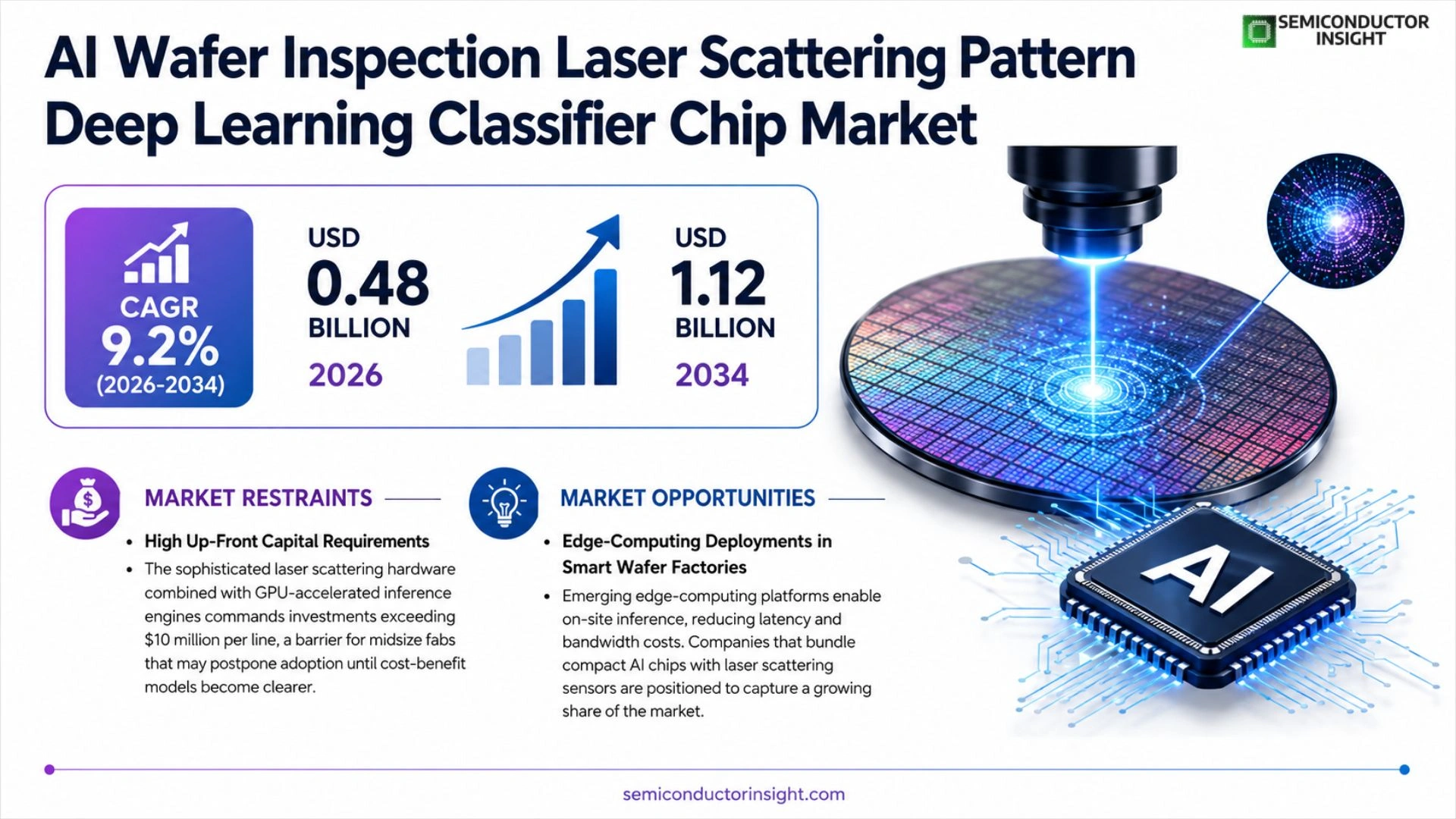
Global AI Wafer Inspection Laser Scattering Pattern Deep Learning Classifier Chip market size was valued at USD 0.45 billion in 2025. The market is projected to grow from USD 0.48 billion in 2026 to USD 1 12 billion by 2034, exhibiting a CAGR of 9.2% during the forecast period.
AI Wafer Inspection Laser Scattering Pattern Deep Learning Classifier chips integrate high‑resolution laser scattering sensors with convolutional neural network accelerators to classify wafer defects in real time. These chips process scattering patterns generated by laser illumination of semiconductor wafers, enabling sub‑micron defect detection that surpasses traditional optical inspection methods.
The market is experiencing rapid growth due to escalating demand for higher yield in advanced node fabs, increased capital expenditure on smart manufacturing, and continuous improvements in deep‑learning inference hardware. Furthermore, collaborations such as the June 2024 partnership between KLA Corp..and NVIDIA to co‑develop optimized inference pipelines are accelerating adoption. Major players including Applied Materials, ASML Holding, and Tokyo Electron are expanding their portfolios with dedicated classifier chips, further fueling market expansion.
MARKET DRIVERS
Rapid Adoption of AI‑Enabled Metrology
AI Wafer Inspection Laser Scattering Pattern Deep Learning Classifier Chip Market is being propelled by semiconductor fabs that are integrating AI‑driven metrology to cut defect‑review times by up to 40%. Advanced deep‑learning classifiers enable real‑time pattern recognition, which translates into higher yields and lower cost of ownership for manufacturers.
Increasing Demand for High‑Precision Lithography
As logic nodes advance below 5 nm, the tolerance for wafer‑level variations shrinks dramatically. Companies are deploying laser scattering inspection systems that leverage deep learning to detect sub‑nanometer anomalies, driving an estimated 12% CAGR through 2030.
➤ “Deep‑learning classifiers reduce false‑positive rates by nearly 30% compared with traditional rule‑based systems,”
These efficiency gains are reinforced by strong capital expenditure cycles in leading foundries, creating a virtuous loop of technology upgrades and market expansion.
MARKET CHALLENGES
Data Scarcity for Rare Defect Types
Training robust classifiers requires large, labeled datasets. For emerging defect patterns, especially those arising from novel EUV processes, the lack of historic data hampers model accuracy, forcing vendors to invest heavily in synthetic data generation.
Other Challenges
Integration Complexity
Embedding AI inspection modules into existing fab automation suites demands interoperable software stacks and skilled personnel, increasing deployment timelines and operational risk.
MARKET RESTRAINTS
High Up‑Front Capital Requirements
The sophisticated laser scattering hardware combined with GPU‑accelerated inference engines commands investments exceeding $10 million per line, a barrier for midsize fabs that may postpone adoption until cost‑benefit models become clearer.
MARKET OPPORTUNITIES
Edge‑Computing Deployments in Smart Wafer Factories
Emerging edge‑computing platforms enable on‑site inference, reducing latency and bandwidth costs. Companies that bundle compact AI chips with laser scattering sensors are positioned to capture a growing share of AI Wafer Inspection Laser Scattering Pattern Deep Learning Classifier Chip Market, particularly in regions accelerating Industry 4.0 initiatives.
AI Wafer Inspection Laser Scattering Pattern Deep Learning Classifier Chip Market Trends
Rapid Adoption Fueled by Yield Pressures
The market recorded a valuation of US $0.45 billion in 2025 and is projected to rise to US $1.12 billion by 2034, reflecting a steady compound growth of roughly 9 % per annum. This expansion is anchored in the semiconductor industry’s relentless push for sub‑micron defect detection, where laser‑based scattering combined with deep‑learning inference delivers real‑time classification that outperforms conventional optical inspection. Fab operators are allocating increasing capital toward smart manufacturing platforms that embed these classifier chips, recognizing that higher yield translates directly into cost savings at advanced nodes.
Other Trends
Strategic Partnerships Accelerate Innovation
Collaborations are reshaping the competitive landscape. In June 2024, KLA Corp. announced a joint development effort with NVIDIA to co‑design inference pipelines optimized for wafer‑inspection workloads. Such alliances reduce time‑to‑market for new hardware generations and enable software ecosystems that leverage pretrained convolutional models. Meanwhile, industry leaders including Applied Materials, ASML Holding, and Tokyo Electron are expanding their product suites with dedicated classifier ASICs, creating a virtuous cycle of technology rollout and customer adoption.
Hardware Integration and Cost Efficiency
As chip manufacturers embed scattering sensors directly into inspection heads, the overall system bill of materials declines while performance improves. Integrated designs eliminate the latency associated with external processing units, allowing defect classification within the same optical path used for imaging. Cost analyses indicate that the total ownership expense of a fully integrated AI‑enabled inspection line can be reduced by up to 15 % compared with legacy configurations, making the technology attractive for mid‑size fabs seeking to upgrade without extensive capital outlay.
COMPETITIVE LANDSCAPE
Key Industry Players
AI Wafer Inspection Laser Scattering Pattern Deep Learning Classifier Chip Market Overview
The market is anchored by a small cohort of vertically integrated semiconductor equipment leaders. Applied Materials, ASML Holding, and Tokyo Electron dominate the ecosystem by supplying end‑to‑end laser‑scattering inspection platforms that embed proprietary deep‑learning inference accelerators. Their extensive fab‑customer bases enable rapid scale‑up of classifier chips, driving the projected CAGR of 9.2 % toward a $1.12 billion market by 2034. Strategic alliances—such as the 2024 KLA‑NVIDIA partnership—reinforce the premium positioning of these incumbents, allowing them to capture the majority of revenue from advanced‑node fabs seeking sub‑micron defect detection.
Beyond the core triad, a second tier of specialist and cross‑industry players is expanding the technology frontier. KLA Corp. contributes differentiated scattering optics, while NVIDIA supplies GPU‑based inference engines that are being co‑designed into inspection ASICs. Intel, Samsung Electronics, and TSMC are integrating classifier chips into their own manufacturing lines to improve yield. Lam Research, Advantest, Siemens‑Mentor (formerly Mentor Graphics), GlobalFoundries, Cadence Design Systems, and IBM Research round out the competitive set, each offering niche sensor designs, algorithmic expertise, or fab‑level customization that address specific process nodes or defect classes.
List of Key AI Wafer Inspection Laser Scattering Pattern Deep Learning Classifier Chip Companies Profiled
- Applied Materials
- Applied Materials
- ASML Holding
- ASML Holding
- Tokyo Electron
- Tokyo Electron
- KLA Corp.
- KLA Corp.
- NVIDIA
- NVIDIA
- Intel
- Samsung Electronics
- TSMC
- Lam Research
- Advantest
- Siemens‑Mentor (Mentor Graphics)
- GlobalFoundries
- Cadence Design Systems
- IBM Research
Segment Analysis:
| Segment Category | Sub-Segments | Key Insights |
| By Type |
|
Hardware‑Accelerated Classifier Chips
|
| By Application |
|
Advanced Node Wafer Defect Detection
|
| By End User |
|
Semiconductor Foundries
|
| By Integration Level |
|
Fab‑Level Integrated Platforms
|
| By Competitive Landscape |
|
Incumbent Tool Suppliers
|
Regional Analysis: AI Wafer Inspection Laser Scattering Pattern Deep Learning Classifier Chip Market
Semiconductor fabs across the United States rapidly integrate laser scattering techniques with AI‑driven analytics, enabling real‑time defect detection. Collaborative research programs between universities and industry accelerate the rollout of next‑generation deep‑learning classifiers, shortening the time from prototype to production.
Federal agencies provide clear guidelines for data security and intellectual property protection in AI‑enhanced inspection tools. Incentives such as tax credits for advanced manufacturing technologies further stimulate adoption across the region.
Companies like KLA‑Tencor, Applied Materials, and several specialized AI startups dominate the market, forming strategic alliances that blend hardware expertise with cutting‑edge deep‑learning algorithms for wafer defect classification.
Venture capital and corporate R&D funds increasingly target AI‑driven inspection platforms, reflecting confidence in the technology’s ability to improve yield and lower production costs in high‑value chip segments.
Europe
European semiconductor hubs in Germany, the Netherlands, and France are cultivating expertise in AI‑based wafer inspection. Collaborative EU frameworks promote standardization of laser scattering data formats, facilitating cross‑border technology transfer. Leading firms focus on integrating deep‑learning classifiers with existing lithography inspection lines, emphasizing sustainability by reducing waste through more accurate defect prediction. While adoption lags slightly behind North America, strong governmental support and a robust supply chain keep Europe competitive in AI Wafer Inspection Laser Scattering Pattern Deep Learning Classifier Chip Market.
Asia‑Pacific
The Asia‑Pacific region, anchored by Taiwan, South Korea, and China, displays vigorous growth in wafer inspection capabilities. Massive fab expansions drive demand for high‑throughput laser scanning systems paired with AI classifiers that can handle diverse device architectures. Regional players prioritize cost‑effective solutions, often co‑developing algorithms with local AI research institutes. Although regulatory environments differ, the sheer volume of production ensures the region becomes a pivotal consumer of advanced inspection technologies.
South America
South America’s semiconductor activities remain modest but are gaining momentum through partnerships with North American technology providers. Emerging markets in Brazil and Chile are investing in pilot projects that test AI‑enhanced laser scattering inspection in low‑volume specialty fabs. The focus is on skill development and establishing localized data sets to train deep‑learning models, positioning the region for incremental growth in the broader market.
Middle East & Africa
In the Middle East & Africa, nascent semiconductor initiatives are leveraging AI Wafer Inspection solutions to accelerate technology transfer. Strategic investments from sovereign wealth funds aim to build state‑of‑the‑art inspection labs in the United Arab Emirates and South Africa. Emphasis is placed on capacity building and adapting deep‑learning classifiers to regional manufacturing constraints, laying the groundwork for future participation in the global market.
Report Scope
This market research report provides a comprehensive analysis of the AI Wafer Inspection Laser Scattering Pattern Deep Learning Classifier Chip Market , covering the forecast period 2026–2034. It offers detailed insights into market dynamics, technological advancements, competitive landscape, and key trends shaping the industry.
Key focus areas of the report include:
- Market Overview: The report begins with an overview outlining its current market scenario, key growth indicators, and industry transformation drivers. It discusses macroeconomic factors, demand–supply balance, regulatory landscape, and the strategic role of semiconductors in powering advancements across industries such as automotive, telecommunications, consumer electronics, and industrial automation.
- Market Size & Forecast: Historical data and future projections for revenue, unit shipments, and market value across major regions and segments.
- Segmentation Analysis: Detailed breakdown by product type, technology, application, and end-user industry to identify high-growth segments and investment opportunities.
- Regional Insights: Insights into market performance across North America, Europe, Asia-Pacific, Latin America, and the Middle East & Africa, including country-level analysis where relevant.
- Competitive Landscape: Profiles of leading market participants, including their product offerings, R&D focus, manufacturing capacity, pricing strategies, and recent developments such as mergers, acquisitions, and partnerships.
- Technology Trends & Innovation: Assessment of emerging technologies, integration of AI/IoT, semiconductor design trends, fabrication techniques, and evolving industry standards.
- Market Drivers & Restraints: Evaluation of factors driving market growth along with challenges, supply chain constraints, regulatory issues, and market-entry barriers.
- Stakeholder Insights: Insights for component suppliers, OEMs, system integrators, investors, and policymakers regarding the evolving ecosystem and strategic opportunities.
Primary and secondary research methods are employed, including interviews with industry experts, data from verified sources, and real-time market intelligence to ensure the accuracy and reliability of the insights presented.
FREQUENTLY ASKED QUESTIONS:
What is the current market size of AI Wafer Inspection Laser Scattering Pattern Deep Learning Classifier Chip Market?
-> AI Wafer Inspection Laser Scattering Pattern Deep Learning Classifier Chip market size is projected to grow from USD 0.48 billion in 2026 to USD 1 12 billion by 2034
Which key companies operate in AI Wafer Inspection Laser Scattering Pattern Deep Learning Classifier Chip Market?
-> Key players include Applied Materials, ASML Holding, and Tokyo Electron, among others.
What are the key growth drivers?
-> Key growth drivers include escalating demand for higher yield in advanced node fabs, increased capital expenditure on smart manufacturing, and continuous improvements in deep‑learning inference hardware.
Which region dominates the market?
-> The provided reference does not specify a dominant geographic region for this market.
What are the emerging trends?
-> Emerging trends include strategic collaborations such as the June 2024 partnership between KLA Corp. and NVIDIA, and the development of optimized AI inference pipelines for wafer inspection.
Get Sample Report PDF for Exclusive Insights
Report Sample Includes
- Table of Contents
- List of Tables & Figures
- Charts, Research Methodology, and more...


