Chiplet Gamble: How Breaking Chips Apart Finally Paid Off in 2026
For decades, the dream of every chip designer was to put everything on one piece of silicon. A single, monolithic slab that held the processor, the memory controller, the graphics engine, the works. That was the recipe for speed, and for a long time it worked beautifully. But around the time the industry started pushing past 7 nanometres, the economics of gigantism began to sour. Making a single enormous die on the most advanced node got eye-wateringly expensive, and when a tiny defect crept in – which happened more often than anyone liked – you had to throw the whole thing away.
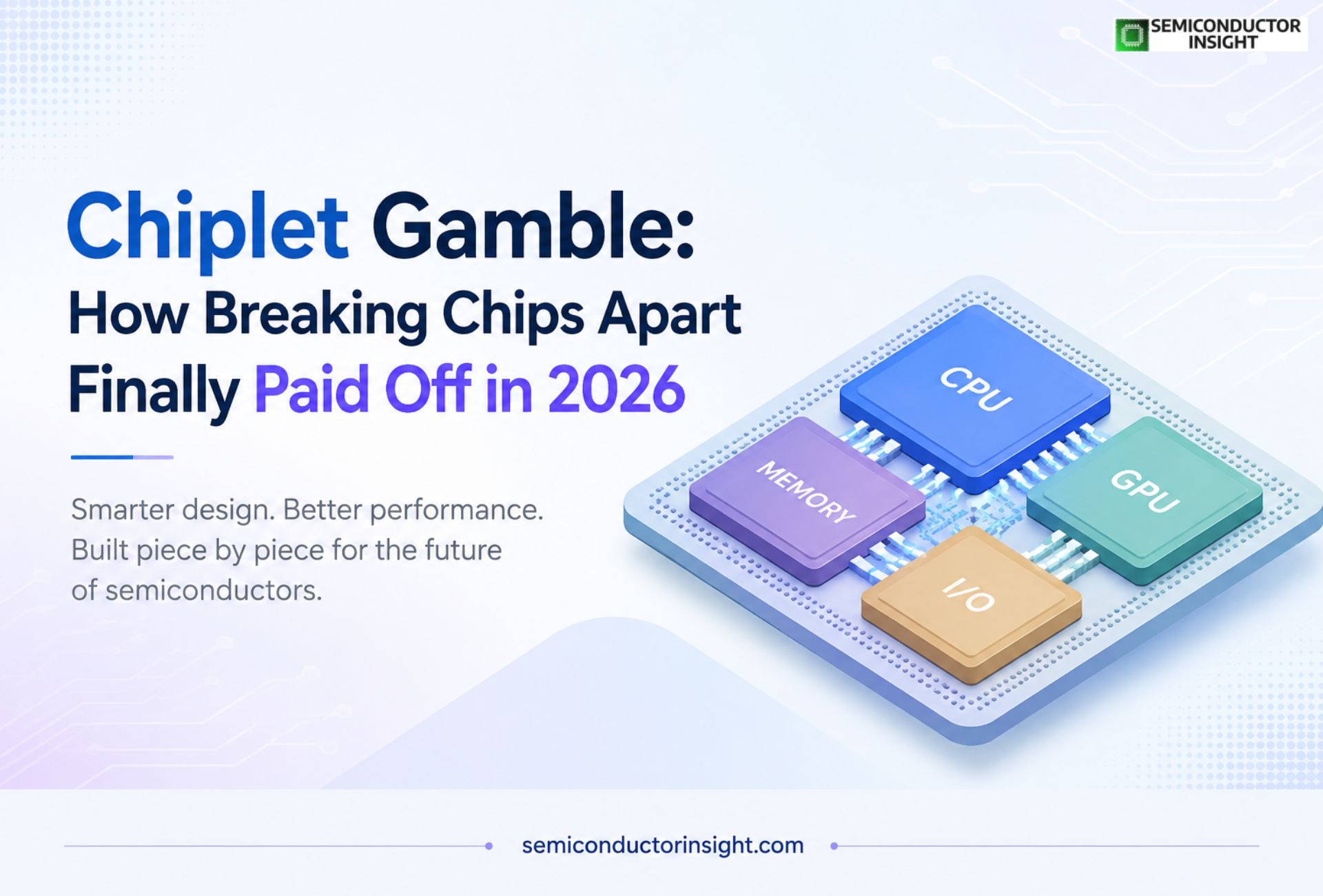
By 2026, the industry had found a different path, and it is one that sounds almost too simple to be revolutionary. Instead of building one huge chip, you build several smaller ones, each optimised for a specific job, and then stitch them together inside a single package. These are chiplets. And what started as a compromise is now turning into the semiconductor world’s most important strategy shift in a generation.
The Lego-block approach to silicon
The basic insight behind chiplets is that not every function needs the same expensive, bleeding-edge manufacturing process. The core processor logic, yes – that benefits from the latest 3‑nanometre or even 2‑nanometre technology. But the input/output block that talks to memory and PCIe lanes? That works perfectly well on a cheaper, mature 12‑nanometre process. Trying to cram both onto the same die meant either spending more money than necessary or compromising on performance.
Chiplets let you break those functions apart, build each piece on the node that makes sense, and then connect them using a high-speed interface. Think of it as designing with Lego blocks rather than carving a statue from a single block of marble. If one chiplet fails testing, you replace it. If you want to upgrade the processor core next year, you design a new chiplet and leave the rest of the package untouched. This modularity is what makes the approach so attractive, and it is why almost every major semiconductor company has now placed a bet on it.
The quiet standard that made it all possible
For years, chiplet interconnects were proprietary. AMD had its own secret sauce, Intel had another, and if you were a smaller company hoping to mix and match, you were out of luck. Then came UCIe – the Universal Chiplet Interconnect Express – which did for chiplet communication what USB once did for computer peripherals. It created an open standard that allows chiplets from different designers and different fabs to talk to one another reliably.
By mid-2026, UCIe 2.0 was showing up in real silicon. At the Design Automation Conference in San Francisco this June, engineers demonstrated test chips running UCIe links at 36 gigabits per second per lane, a speed that makes disaggregating even memory-hungry workloads entirely practical. What this meant on the ground was that a fabless startup could now buy a standard UCIe interface block, design a compute chiplet on a cutting-edge node, commission a separate I/O chiplet from another foundry, and expect the two to shake hands without drama. That lowered the barrier to entry enormously and opened the door to a wave of chiplet-based innovation that was previously reserved for the industry’s giants.
How the heavyweights are playing their hands
AMD was the poster child for early chiplet adoption, and by 2026 it is reaping the rewards. The company’s EPYC server processors separate the high-performance compute dies from a central I/O die built on an older, cheaper process. During an earnings call in May, the company’s chief technology officer let slip that reusing chiplets across multiple product lines had cut development costs by about thirty percent on some server platforms. That kind of saving turns a technology choice into a hard-nosed business advantage.
Intel, after a period of public hand-wringing, has gone all in as well. The company’s Meteor Lake chips, which arrived in late 2023, were Intel’s first wide deployment of its Foveros packaging technology that stacks chiplets vertically. By 2026, Intel Foundry is actively selling advanced packaging services to external customers, with a pitch that essentially says: bring us your chiplets, we’ll put them together. For a company that once kept its factories almost entirely for its own designs, that is a remarkable pivot.
Then there is TSMC, which holds much of the advanced packaging capacity the industry depends on. Its CoWoS technology – Chip-on-Wafer-on-Substrate – is the backbone of NVIDIA’s data-centre GPUs, which are themselves chiplet-based in their latest Blackwell architectures. Early this year, TSMC’s quarterly earnings revealed that advanced packaging revenue had jumped forty-five percent year-on-year, driven almost entirely by chiplet designs for AI and high-performance computing. The company is racing to add more capacity in Taiwan and a new plant in Japan, but demand still runs ahead of supply. The bottleneck tells its own story.
AI supercomputers are forcing the shift
The explosion of artificial intelligence has been the single biggest accelerant for chiplets. Training large language models and running generative AI workloads requires a staggering amount of compute and memory bandwidth. A monolithic chip runs into a hard physical wall called the reticle limit – the largest single die a lithography machine can print, roughly 800 square millimetres. Beyond that, you simply cannot build a single chip.
Chiplets sidestep that limit. NVIDIA’s Blackwell Ultra platform, announced at GTC in March, uses two enormous compute tiles connected by a blisteringly fast NVLink interconnect. It acts like one giant chip while being physically several smaller ones. This design not only circumvents the reticle limit but also allows NVIDIA to mix and match compute and memory chiplets for different customer needs. Hyperscalers like Amazon and Google are following suit with their own custom AI chips, increasingly built on chiplet architectures and often using UCIe internally.
Better yields, fewer headaches
Chiplets also solve a manufacturing problem that has bedevilled the industry as nodes shrink. When a monolithic chip has a defect anywhere, you lose the entire die. With chiplets, only the faulty piece is scrapped. The rest of the package can still be sold. This yield improvement alone can make the difference between a profitable product line and a money pit. But it does mean that testing becomes more complicated. Each chiplet must be proven good before assembly, a process called known-good-die testing. The industry has responded with new inspection tools, and in February, KLA Corporation rolled out a metrology platform specifically for chiplet interposers, claiming a forty percent improvement in inspection throughput.
Governments lean in
Governments have noticed that controlling advanced packaging is as strategically important as owning leading-edge fabs. The U.S. CHIPS Act set aside billions for packaging, and in April 2026 the Commerce Department awarded $1.6 billion to a consortium building a national advanced packaging pilot line in upstate New York. The goal is to reduce dependence on Asian facilities. Europe, Japan, and India are all pursuing similar initiatives. Chiplet technology is now squarely in the realm of economic and national security.
What all this means for a market that is hard to size but impossible to ignore
The chiplet market does not exist as a neat category on a spreadsheet. It is an ecosystem – design tools, interface IP, advanced packaging services, interposers, testing – and it is growing rapidly. The best proxy may be advanced packaging revenue, which crossed $40 billion globally in 2025 and is expected to keep climbing at double-digit rates through the decade’s end, according to industry association figures. The growth is being pulled by AI, data centres, and the automotive shift to modular architectures.
In 2026, the conversation has shifted completely. A decade ago, chiplets were seen as a concession – something you did when scaling stopped working. Now they are increasingly viewed as the smarter way to design chips from the start. As one Intel executive put it at a conference in May, the monolithic era is over. That may sound bold, but a tour of any advanced packaging facility today would confirm it. The factories that once printed ever-larger single chips are now assembling ever-more intricate collections of smaller ones, and the results are the processors that will power the next wave of computing. Breaking things apart, it turns out, was the best way to keep building.
Explore our latest report: https://semiconductorinsight.com/report/chiplet-ic-market/
Comments (0)