
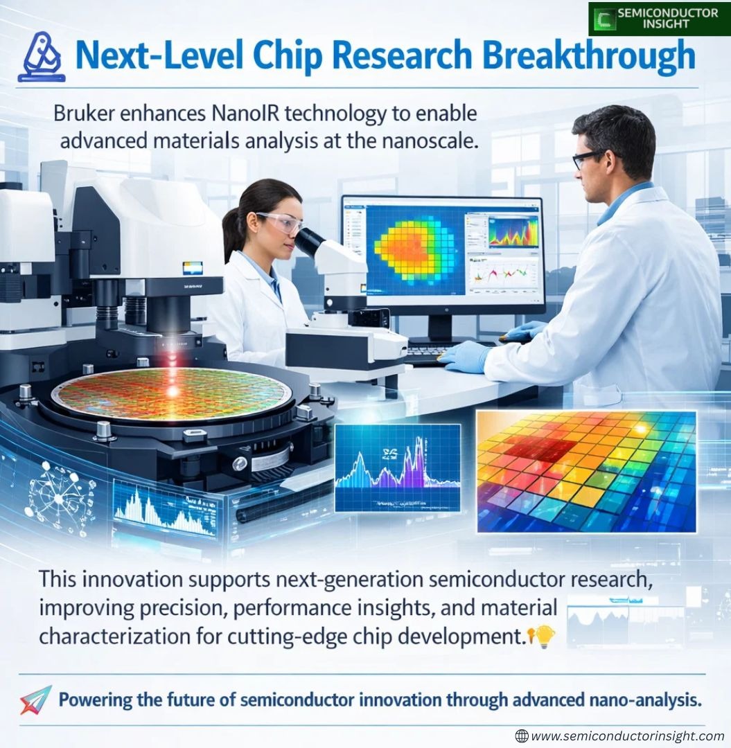
Bruker Advances NanoIR Capabilities to Support Next-Generation Semiconductor Research
Bruker Corporation has announced the accelerated development of its photothermal AFM-IR (nanoIR) spectroscopy capabilities, aimed at addressing growing research challenges in the semiconductor industry as device architectures become increasingly complex and miniaturized.
The company, a leading supplier of nanoscale infrared spectroscopy solutions, is expanding the application of AFM-IR beyond contamination analysis into critical areas such as EUV photoresist development, advanced materials for transistor scaling, and nanoscale surface functionalization for emerging device applications.
As part of this initiative, Bruker has partnered with imec under a Joint Development Project (JDP). The collaboration includes the installation of Bruker’s Dimension IconIR system to evaluate the role of nanoscale chemical characterization in understanding material behavior and interface interactions that directly impact semiconductor process development and device performance.
Albert Minj, senior researcher at Imec and project lead of the JDP, stated, Metrology requirements for advanced semiconductor research are evolving rapidly, and together with Bruker will assess how nanoIR technology can help address emerging requirements in nanoscale materials characterisation.
Get Instant Access to Our Latest Relevant Research Highlights: https://semiconductorinsight.com/report/afm-for-semiconductor-market/
LinkedIn Semiconductor News:
Next-Level Chip Research: Bruker Enhances NanoIR for Advanced Materials Analysis
A strategic push toward next-generation semiconductor innovation Bruker Corporation is accelerating the development of its photothermal AFM-IR (nanoIR) spectroscopy capabilities to address increasing complexity in chip architectures.
As device scaling advances, Bruker is expanding nanoIR applications beyond contamination analysis into critical research areas shaping future semiconductors, including EUV photoresist development, advanced transistor materials, and nanoscale surface functionalization.
Metrology requirements for advanced semiconductor research are evolving rapidly, and together with Bruker will assess how nanoIR technology can help address emerging requirements in nanoscale materials characterisation, commented Albert Minj, senior researcher at Imec and project lead of the JDP.
In collaboration with imec, Bruker has deployed its Dimension IconIR system to evaluate how nanoscale chemical characterization can unlock deeper insights into material behavior and interface performance.
The strategic advantage behind this:
- Enables label-free chemical analysis at sub-5 nm resolution
- Supports EUV lithography and next-gen device development
- Enhances understanding of complex material interactions
- Addresses evolving metrology demands in semiconductor R&D
Access the Latest Insights from Our Newly Released Related Report: https://semiconductorinsight.com/report/afm-for-semiconductor-market/
#SemiconductorIndustry #Nanotechnology #Metrology #ChipInnovation #AdvancedMaterials #EUV #NanoIR #R&D #TechInnovation #Electronics #FutureOfChips #ScientificInnovation #HighTech

Comments (0)