
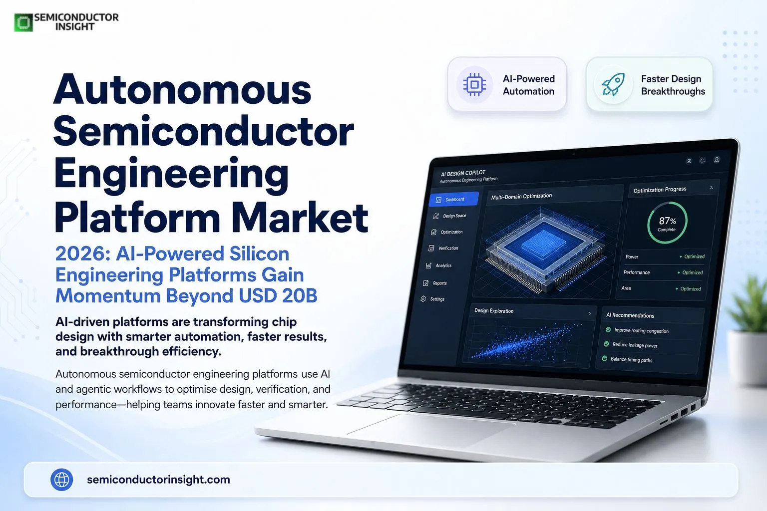
Autonomous Semiconductor Engineering Platform Market 2026: AI-Powered Silicon Engineering Platforms Gain Momentum Beyond USD 20B
The semiconductor industry continues pushing boundaries as design complexity for AI chips, automotive systems, and high-performance computing grows exponentially.
Autonomous engineering platforms and systems that leverage AI, machine learning, and agentic workflows have moved from experimental stages to practical deployment in chip development flows. These platforms help engineering teams navigate massive design spaces, automate routine decisions, and focus human expertise on higher-level challenges.
Understanding Core Technologies in Daily Chip Design
- At the foundation of these platforms lies reinforcement learning and other AI methods that explore optimisation possibilities far beyond traditional manual approaches.
- Synopsys introduced DSO.ai in 2020 as one of the early commercial autonomous AI applications for chip design. By 2023, it had contributed to over 100 commercial chips, demonstrating real production impact.
- The tool uses reinforcement learning to optimise power, performance, and area (PPA) across logical and physical domains.
- Cadence offers its Cadence.AI suite with tools like Cerebrus for digital design optimisation and Verisium for verification. These systems incorporate agentic AI workflows that reduce engineering time on complex system-on-chip (SoC) Engineers report that such platforms allow them to evaluate more design variants while maintaining control over final architectural choices.
High-Performance Results from Strategic Implementations
Google DeepMind’s AlphaChip has shown impressive results in accelerating chip layout processes. The reinforcement learning-based method designs superhuman layouts in hours instead of weeks, and its techniques now support multiple generations of Google’s Tensor Processing Units. This approach has influenced broader thinking about AI assistance in physical design stages.
In one documented verification case involving network processors, AI-augmented systems identified over 1,300 unique test scenarios that traditional methods missed, uncovering dozens of critical bugs before silicon production. Such outcomes highlight how autonomous platforms complement human oversight rather than replace it.
Data Points on R&D Investment and Industry Scale
- S. semiconductor manufacturing companies performed $47.4 billion in R&D in 2021, with strong company-funded portions concentrated in key states. By 2024, overall U.S. semiconductor industry R&D reached $62.7 billion, reflecting continued commitment to advanced tools and methodologies. The sector directly employs around 345,000 people in areas including electronic design automation.
- These investments support the development of platforms that address the growing transistor counts and system complexities in modern chips. Engineering teams working on multi-die designs particularly benefit from tools that optimise across chiplets for thermal, signal, and power integrity.
How Do These Platforms Handle Verification Complexity?
Many engineers ask how autonomous platforms manage the verification of advanced designs. Current systems generate test benches, identify corner cases, and even suggest fixes for certain bug classes using large language models and agentic approaches. For instance, frameworks have successfully created SystemVerilog Assertions from natural language descriptions, achieving reasonable accuracy that improves with iterative refinement.
In practice, human experts set high-level intent and constraints while the platform explores detailed implementations. This collaboration has proven effective in reducing verification cycles for processors and accelerators.
Overview of Agentic AI, Multi‑Domain Optimisation, and Public Initiatives
Agentic AI is emerging as a key capability within autonomous semiconductor engineering platforms, enabling software agents to carry out tasks such as circuit validation, RTL optimisation, and proactive debugging. Rather than only reacting to errors, these systems increasingly anticipate issues and propose fixes across the design flow early deployments and conference discussions in 2025 indicate leading firms are already piloting such workflows.
- At the same time, platforms are evolving to support multi‑domain optimisation: integrating analogue, mixed‑signal, and digital design flows so teams can evaluate tradeoffs across domains within a single environment.
- This holistic approach is becoming essential as modern chips combine diverse components for AI inference at the edge and in data centres, where cross‑domain interactions strongly affect power, performance, and area.
- Public policy and collaborative programs are accelerating adoption and innovation in these areas.
- In the U.S., the CHIPS and Science Act has directed substantial funding toward R&D, including initiatives that support advanced design tools; the National Semiconductor Technology Centre is a focal point for public‑private partnerships aimed at strengthening next‑generation design capabilities.
Comparable international efforts likewise prioritise resilient ecosystems and highlight engineering platforms as strategic assets for controlling rising design costs and preserving competitiveness. Together, advances in agentic AI, cross‑domain platform integration, and government backing are driving a shift from fragmented, reactive tools to unified, anticipatory engineering platforms that can handle the complexity of modern semiconductor design.
Traditional EDA vs. Autonomous Platforms
Engineers familiar with conventional flows notice clear differences when transitioning to autonomous platforms. Traditional methods rely heavily on manual iteration and expert rules of thumb. In contrast, AI-driven systems explore trillions of possible design recipes, often achieving better PPA results with less engineering effort.
However, successful adoption requires teams to develop new skills in guiding AI systems and validating their outputs. Many organisations implement hybrid approaches where platforms handle optimisation loops while humans focus on innovation and system-level architecture.
Practical Implementation in Different Sectors
Automotive chip designers use these platforms to meet stringent safety and reliability standards while incorporating AI capabilities for advanced driver assistance. Data centre teams leverage them for custom accelerators that deliver higher efficiency for training and inference workloads.
The platforms also support smaller design teams in exploring custom solutions that were previously out of reach due to resource constraints. This democratization aspect appears in various case examples shared through technical communities.
Lastly, for more in-depth information, don’t forget to read our most recent exclusive report: https://semiconductorinsight.com/report/autonomous-semiconductor-engineering-platform-market/
Sustainability and Long-Term Engineering Considerations
As platforms become more capable, discussions around energy-efficient design gain prominence. Autonomous optimisation can target lower power consumption from the earliest stages, contributing to greener computing overall. Teams increasingly factor in lifecycle aspects when setting platform parameters.
Ongoing education remains vital. Universities and industry programs are adapting curricula to prepare the next generation of engineers who will work alongside these intelligent systems.
Autonomous Semiconductor Engineering Platform Market continues to mature through practical deployments that deliver measurable improvements in design quality and speed. As more organisations integrate these tools, the collective knowledge about best practices grows, benefiting the entire semiconductor ecosystem.

Comments (0)