ASML and SK hynix Unveil First Commercial High-NA EUV System, Driving Next-Gen Photomask Demand
The semiconductor industry is undergoing a massive transformation driven by surging demand for smaller, faster, and more power-efficient devices. At the heart of this revolution lies one of the most critical tools for chip fabrication the photomask. Among the different mask technologies, Quartz Chromium Masks have retained their dominance due to their precision, stability, and adaptability to both deep ultraviolet (DUV) and extreme ultraviolet (EUV) lithography techniques.
In 2024, the Quartz Chromium Mask market was valued at USD 5,288 million. With continuous advancements in semiconductor lithography, rising investment in High-NA EUV systems, and new developments in mask qualification, the market is projected to reach USD 7,440 million by 2032, growing at a CAGR of 5.1% during the forecast period.
Access Your Free Sample Report- Quartz Chromium Mask Market
1. The Strategic Role of Quartz Chromium Masks in Semiconductor Manufacturing
Quartz Chromium Masks are specialized glass plates coated with chromium patterns that act as templates for transferring circuit designs onto semiconductor wafers. Their high optical transparency, thermal resistance, and durability make them the gold standard for advanced lithography processes.
Key applications include:
- Memory devices (DRAM, NAND, and emerging memories): Precise mask performance is crucial for multi-layer structures.
- Logic devices (CPUs, GPUs, and AI accelerators): Advanced nodes below 3 nm require ultra-fine resolution masks.
- Specialty semiconductors (RF, automotive, sensors): Diverse applications demand varying mask qualities, from i-line to EUV.
With Moore’s Law continuing to push physical limits, Quartz Chromium Masks are evolving to meet stricter requirements, from minimizing defects to enabling complex resolution enhancement techniques (RET) such as Inverse Lithography Technology (ILT) and optical proximity correction (OPC).
2. Market Overview and Growth Projections
The Quartz Chromium Mask market demonstrates a steady growth trajectory supported by multiple demand drivers:
- Market Valuation (2024): USD 5,288 million
- Projected Valuation (2032): USD 7,440 million
- CAGR (2024–2032):1%
Growth Drivers:
- EUV adoption: As EUV moves into mainstream logic and memory production, new generations of Quartz Chromium Masks are required.
- High-NA lithography: The transition to 0.55 NA systems increases demand for ultra-precise mask substrates.
- Global chip shortages and fab expansions: Companies such as TSMC, Intel, and Samsung are investing billions in new fabs, driving parallel demand for photomasks.
- AI and HPC growth: Accelerated demand for GPUs and AI accelerators translates into more advanced mask requirements.
Regional Market Insights:
- Asia-Pacific (APAC): Largest market share, led by Taiwan, South Korea, Japan, and China.
- North America: Driven by U.S. investments under the CHIPS Act and Intel’s roadmap.
- Europe: Anchored by ASML and Zeiss in lithography innovation, supported by EU funding.
Download Sample Report PDF- Quartz Chromium Mask Market
3. Recent Developments Shaping the Industry
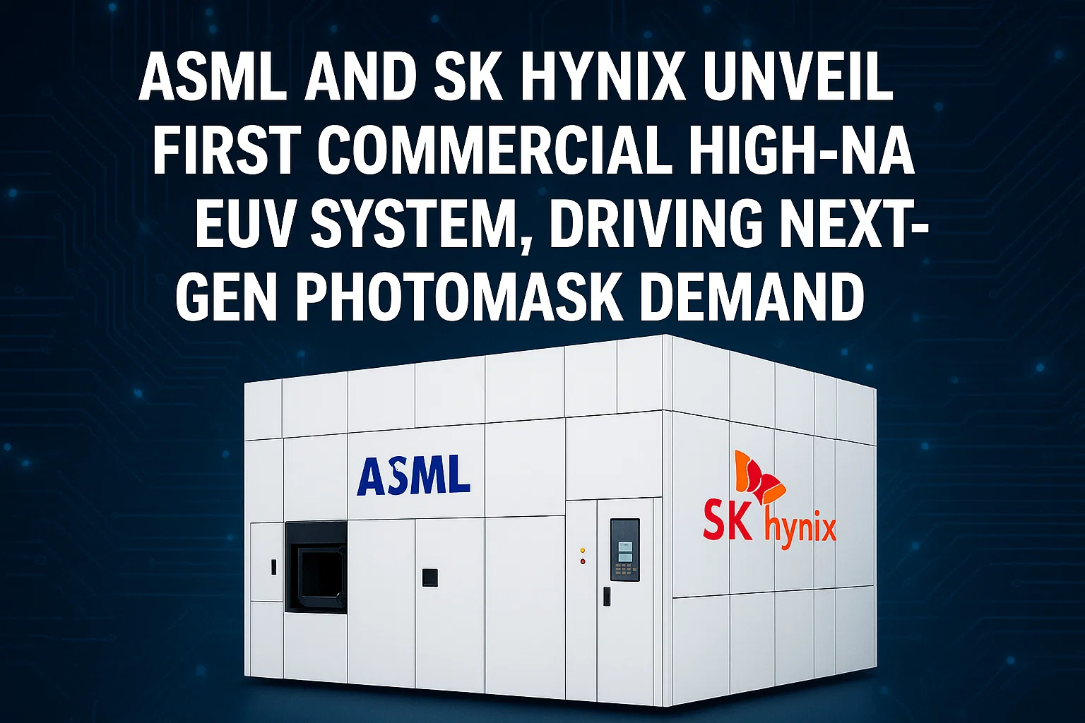
3.1 ASML and SK Hynix Build the First High-NA EUV System
In 2025, ASML and SK Hynix assembled the first commercial High-NA EUV system at SK hynix’s M16 fab in South Korea. This landmark installation of the Twinscan NXE:5200B tool enables finer patterning for sub-2 nm logic and DRAM production.
Impact on Quartz Chromium Masks:
- Requires new generations of quartz substrates with tighter defect control.
- Drives demand for advanced chromium mask blanks optimized for higher NA optics.
- Spurs collaboration across mask makers (like DNP and Tekscend) to prepare High-NA ready masks.
3.2 ZEISS Unveils AIMS EUV 3.0 for Mask Qualification
ZEISS recently launched the AIMS® EUV 3.0 system, capable of tripling mask throughput compared to its predecessor. This solution allows semiconductor companies to rapidly qualify masks for both Low-NA and High-NA EUV applications.
Industry Significance:
- Reduces bottlenecks in mask inspection and defect verification.
- Ensures that chromium-based photomasks meet defect-free standards before wafer exposure.
- Improves fab productivity by shortening mask validation timelines.
3.3 Tekscend Photomask’s IPO
Formerly known as Toppan Photomask, Tekscend Photomask announced a Tokyo IPO, aiming for a valuation of nearly USD 2 billion. This move reflects investor confidence in the growing importance of photomasks in advanced chip manufacturing.
Implications for the Market:
- IPO proceeds expected to expand mask R&D, especially for EUV and High-NA readiness.
- Signals a trend of mask makers seeking independent growth and capital injection to meet global demand.
3.4 Samsung Outsources Photomask Production
In a surprising shift, Samsung began outsourcing lower-end photomasks for i-line and KrF processes, while keeping advanced ArF and EUV masks in-house.
Market Insights:
- Outsourcing frees Samsung’s internal resources to focus on cutting-edge mask development.
- Creates opportunities for external suppliers in the Quartz Chromium Mask ecosystem.
- Indicates a strategic segmentation of mask production based on technology node importance.
3.5 DNP and Next-Gen EUV Photomasks
DNP (Dai Nippon Printing) achieved fine pattern resolution for High-NA EUV photomasks, supplying evaluation samples to chipmakers beyond the 2 nm node.
Importance for Quartz Chromium Masks:
- Reinforces Japan’s leadership in high-precision mask manufacturing.
- Demonstrates readiness for future nodes, supporting both logic and memory customers.
- Expands competition with global mask suppliers, driving innovation and quality improvements.
3.6 Corning Expands Glass Production for EUV Substrates
Corning, a major supplier of glass substrates, announced an expansion of its advanced glass production facilities in the U.S. under CHIPS Act funding.
Relevance to Quartz Chromium Masks:
- Strengthens supply chain resilience for mask blanks.
- Ensures availability of defect-free quartz substrates necessary for EUV and High-NA masks.
- Reduces dependence on overseas suppliers amid geopolitical uncertainties.
3.7 AI-Driven Mask Design and Inverse Lithography
Recent academic and industry breakthroughs highlight AI-assisted mask optimization and Inverse Lithography Technology (ILT). These approaches allow more efficient correction of complex mask patterns, improving imaging fidelity.
Industry Applications:
- Reduces overall mask error rates.
- Cuts computational design costs for advanced masks.
- Accelerates mask readiness for 2 nm and beyond.
4. Opportunities and Challenges in the Quartz Chromium Mask Market
Opportunities:
- EUV and High-NA Era: Masks remain indispensable for every node shrink.
- AI and HPC Chips: Rapid design cycles increase mask set orders.
- Geopolitical Support: CHIPS Act in the U.S. and Japan’s subsidies for photomask innovation provide growth funding.
- Emerging Markets: China’s drive for self-reliance could expand domestic mask demand, even if EUV is restricted.
Challenges:
- Rising Mask Costs: A single advanced mask set can exceed USD 10 million, straining smaller fabless players.
- Defect Management: Even nanometer-scale defects can ruin entire wafers, demanding stringent inspection.
- Supply Chain Fragility: Quartz substrates, chromium coatings, and inspection tools face limited supplier bases.
- Geopolitical Tensions: Export controls (e.g., EUV restrictions to China) reshape mask demand distribution.
Click Here To Download Full Sample Report- Quartz Chromium Mask Market
5. Future Outlook (2025–2032)
The Quartz Chromium Mask industry is set for sustained growth as the semiconductor sector braces for sub-2 nm nodes, AI-driven chips, and advanced memory devices. By 2032, the market will approach USD 7.44 billion, supported by:
- Commercial High-NA adoption around 2026–2028.
- Expansion of advanced fabs by TSMC, Intel, Samsung, and SK Hynix.
- AI-driven mask design workflows reducing cycle times.
- Broader supply chains with contributions from Japan, the U.S., Korea, and Taiwan.
As the market grows from USD 5,288 million in 2024 to USD 7,440 million by 2032 (CAGR 5.1%), the focus will remain on defect control, AI-driven mask design, and scaling High-NA lithography.
Comments (0)