
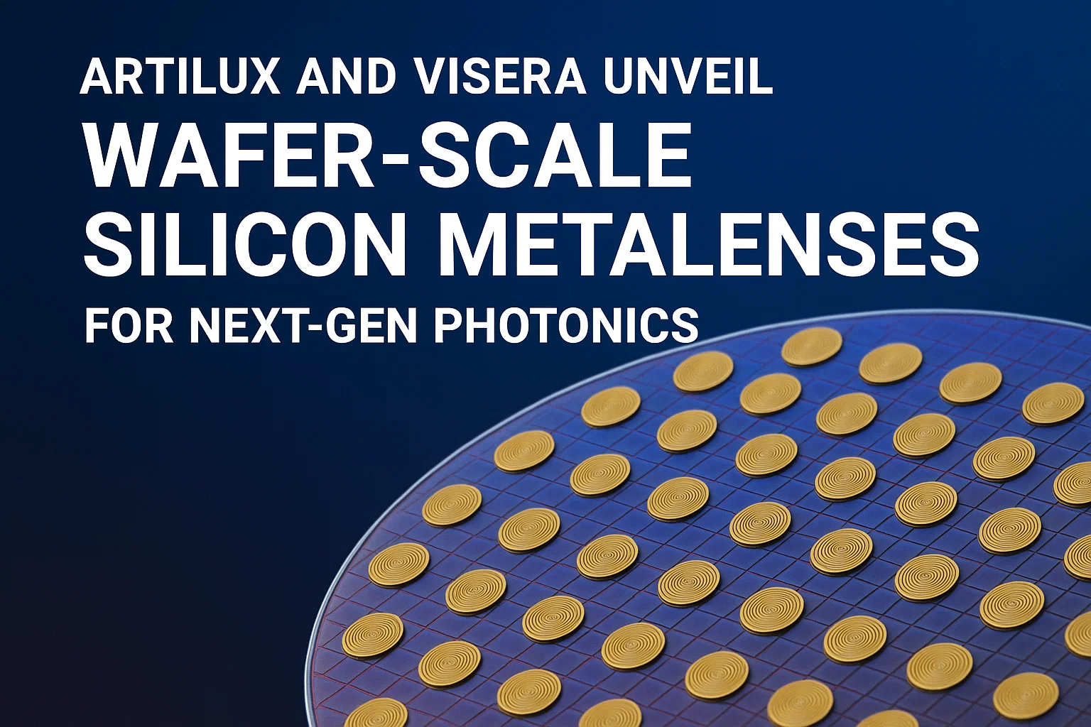
Artilux and VisEra Unveil Wafer-Scale Silicon Metalenses for Next-Gen Photonics
In the ever-accelerating digital age, information is the world’s most valuable currency. Every message, video stream, and financial transaction relies on fast, secure, and reliable communication networks. Optical communication the use of light to transmit data has become the backbone of this infrastructure, enabling everything from undersea cables that carry internet traffic between continents to data centers powering artificial intelligence and cloud computing.
But as demands on our networks grow, traditional optical components face limitations. Conventional lenses, which bend and focus light, are bulky and complex. They take up space, require careful alignment, and have physical constraints that make integration with modern, miniaturized devices challenging.
Enter metalenses: a new class of ultrathin, nanostructured optical devices capable of manipulating light in ways once thought impossible. Instead of relying on curved glass, metalenses use carefully arranged arrays of nanoscale elements often just hundreds of nanometers wide to bend, focus, or scatter light with unprecedented precision. This breakthrough is reshaping the landscape of photonics and, by extension, the future of optical communication.
The commercial promise of this technology is staggering. According to industry analyses, the metalens market for optical communication was valued at USD 29 million in 2024 and is projected to skyrocket to USD 3005 million by 2032, representing a compound annual growth rate (CAGR) of 93.3%. Such explosive expansion underscores not just the excitement in research labs but also the confidence of industry stakeholders in its transformative potential.
Access Your Free Sample Report- Metalens for Optical Communication Market
The Science Behind Metalenses
From Curved Glass to Flat Nanostructures
Traditional lenses rely on the principle of refraction: as light passes through a curved surface, it bends according to Snell’s law, converging to a focal point. While this principle has served humanity well for centuries from eyeglasses to telescopes it comes with drawbacks. Bulk, weight, and manufacturing costs make scaling difficult, particularly as devices become smaller and more integrated.
Metalenses, by contrast, are flat. Instead of shaping the lens itself, they use metasurfaces: engineered arrays of nanoscale structures that interact with incoming light at the subwavelength level. Each nanostructure can be designed to impart a specific phase, amplitude, or polarization shift to the light. By carefully arranging millions of these elements, researchers can create a lens that bends light just like or better than traditional optics, but on a sheet thinner than a human hair.
Why Metalenses Matter in Optical Communication
For optical communication systems, size and efficiency are paramount. Whether coupling light into a fiber, steering beams in free-space optical (FSO) links, or miniaturizing transceiver modules in data centers, every millimeter counts. Metalenses offer:
- Miniaturization: Ultraflat designs reduce size and weight, perfect for compact photonic circuits.
- Integration: Compatible with CMOS fabrication, enabling on-chip photonics.
- Advanced control: Tailored manipulation of wavelength and polarization, useful for multiplexing signals.
- Broadband operation: Emerging achromatic designs can cover full telecom bands (1.25–1.65 μm).
These unique capabilities are driving both academic curiosity and industrial investment.
Recent Research and Technological Developments
1. Scaling Up: Large-Area Metalens Manufacturing
One of the biggest barriers to commercialization has been scalability. Metalenses require nanostructures patterned with extreme precision, historically achievable only through costly and slow electron-beam lithography. That is changing.
- POSTECH (Korea) developed a method using deep UV photolithography the same process used in semiconductor manufacturing to fabricate large-area metalenses. This breakthrough slashed production costs by nearly 1,000 times compared to earlier methods. It opens the door to mass production of high-quality lenses suitable for telecom applications.
- Artilux and VisEra announced the fabrication of metalenses on 12-inch silicon wafers. Wafer-scale production not only improves yield and consistency but also aligns perfectly with existing CMOS photonics, a critical step for integrating metalenses into data center transceivers and optical interconnects.
Together, these advances are transforming metalenses from laboratory curiosities into industrially viable products.
2. Simplifying Design: Reduced Phase-Delay Requirements
Another breakthrough came from Samsung and POSTECH, who introduced a two-third wavelength phase-delay metalens. Traditional designs require a full wavelength phase shift, which demands tall nanostructures with aspect ratios as high as 1:10. These are mechanically fragile and prone to fabrication errors.
By achieving the same focusing effect with only two-thirds of the wavelength phase delay, the team reduced aspect ratios to ~1:5, significantly improving durability, manufacturability, and yield. This makes metalenses more practical for high-volume optical communication systems where reliability is critical.
3. Achromatic Metalenses: Tackling Chromatic Aberration
One challenge in optical communication is the use of multiple wavelengths (WDM systems). Traditional metalenses tend to be wavelength-specific, suffering from chromatic aberration when exposed to broadband light.
Recent innovations are addressing this:
- Researchers developed achromatic metalenses on the end face of single-mode fibers that operate across 25–1.65 μm, directly aligning with telecom bands. This paves the way for fiber-integrated metalenses that can enhance coupling efficiency.
- Samsung and POSTECH also reported achromatic RGB metalenses for imaging applications, showing that nanostructure design principles can be extended across wide spectra. While initially intended for displays, the underlying approach is highly relevant for broadband optical communication.
Download Sample Report PDF- Metalens for Optical Communication Market
4. Integration with Silicon Photonics
The holy grail of optical communication is the seamless integration of all components modulators, detectors, and lenses onto silicon chips. Metalenses are proving increasingly compatible with this vision.
- Artilux + VisEra’s wafer-scale silicon metalenses demonstrate compatibility with existing CMOS processes.
- Researchers are experimenting with GeSi alloys to extend performance into telecom wavelengths.
- Integration promises ultracompact transceiver modules, reducing cost and power consumption in massive data centers.
5. AI-Enhanced Metalenses: Correcting Aberrations with Computation
Even with design advances, some optical imperfections remain. Enter artificial intelligence.
- A team demonstrated metalens-based imaging systems enhanced with deep learning, correcting aberrations and restoring high-resolution images.
- While this was showcased for imaging, the concept could easily translate to optical communication where AI-driven error correction could compensate for residual distortions in fiber coupling or free-space links.
This convergence of nanophotonics and AI may accelerate adoption, providing performance levels unattainable through hardware alone.
6. Free-Space Optical Communication and Spin-Encoded Metalenses
Beyond fiber optics, metalenses are showing promise in free-space optical (FSO) communication a technology gaining attention for satellite internet, drone networks, and secure line-of-sight links.
- Researchers demonstrated silicon-based spin-encoded metalenses capable of producing dual focal points, enabling advanced polarization multiplexing.
- Such designs could double transmission capacity in FSO links or allow simultaneous communication channels, a game-changer for bandwidth-hungry applications like LEO satellite constellations.
Market Outlook: From Niche to Mainstream
The numbers tell a compelling story. In 2024, the metalens market for optical communication stood at a modest USD 29 million. By 2032, it is projected to reach an astonishing USD 3005 million, representing a CAGR of 93.3% one of the highest growth rates of any photonics sector.
Drivers of Growth
- 5G and 6G Networks
The rollout of ultra-fast mobile networks demands advanced backhaul and fronthaul infrastructure, where metalenses can enhance optical transceivers. - Data Centers and Cloud Computing
With AI workloads exploding, hyperscale data centers need more compact, efficient, and high-bandwidth optical interconnects. Metalenses offer exactly that. - Satellite Internet and FSO Links
Companies like SpaceX (Starlink) and Amazon (Kuiper) are investing heavily in LEO constellations. Metalenses could reduce payload weight and enable advanced beam steering. - AR/VR and Wearables
Though not purely communication, the overlap with compact optical modules drives shared innovation and economies of scale. - Defense and Quantum Communication
Secure, high-bandwidth links benefit from the polarization control and miniaturization that metalenses enable.
Regional Leaders
- Asia (South Korea, Taiwan, China, Japan): Strong academic research (POSTECH, Samsung) and semiconductor manufacturing ecosystem.
- United States: Leading in silicon photonics and startup ecosystem.
- Europe: Pioneering academic research in metasurfaces and integration with quantum optics.
Challenges Still Ahead
Despite impressive advances, several hurdles remain before metalenses achieve mainstream deployment in optical communication:
- Optical Efficiency
Many designs still suffer from transmission losses, limiting real-world applicability in telecom. - Manufacturing Yield
Even with wafer-scale approaches, nanostructure precision must be nearly flawless for consistent performance. - Broadband Performance
True achromatic metalenses covering the entire telecom spectrum with minimal loss remain a challenge. - System Integration
Aligning metalenses with fibers, waveguides, or detectors requires sub-micron precision, adding complexity to packaging. - Cost at Scale
While cheaper than before, metalenses must compete with mature, low-cost lens manufacturing.
Click Here To Download Full Sample Report- Metalens for Optical Communication Market
Opportunities and Future Applications
The potential applications are vast, and each represents a billion-dollar opportunity:
- Next-Gen Data Centers: Metalenses could shrink transceiver modules, reduce power use, and boost bandwidth.
- AR/VR and Consumer Electronics: Demand for ultracompact optics will indirectly accelerate metalens production, benefiting telecom.
- LEO Satellite Internet: Lightweight, polarization-multiplexed free-space communication using metalenses could transform space-based broadband.
- Quantum Networks: Metalenses with precise polarization control may enable secure quantum key distribution.
- Defense and Aerospace: Compact, rugged optical components are in high demand for secure and mobile communication platforms.
Metalenses represent more than just a new kind of optical component they are a paradigm shift in how we manipulate light. Over the past two years, breakthroughs in large-area manufacturing, achromatic design, phase-delay reduction, and AI integration have propelled them closer to commercialization in optical communication.
The market projections speak volumes: from USD 29 million in 2024 to USD 3005 million by 2032, with a CAGR of 93.3%. Such growth is rare, signaling not just incremental improvement but a transformative wave in photonics.

Comments (0)