
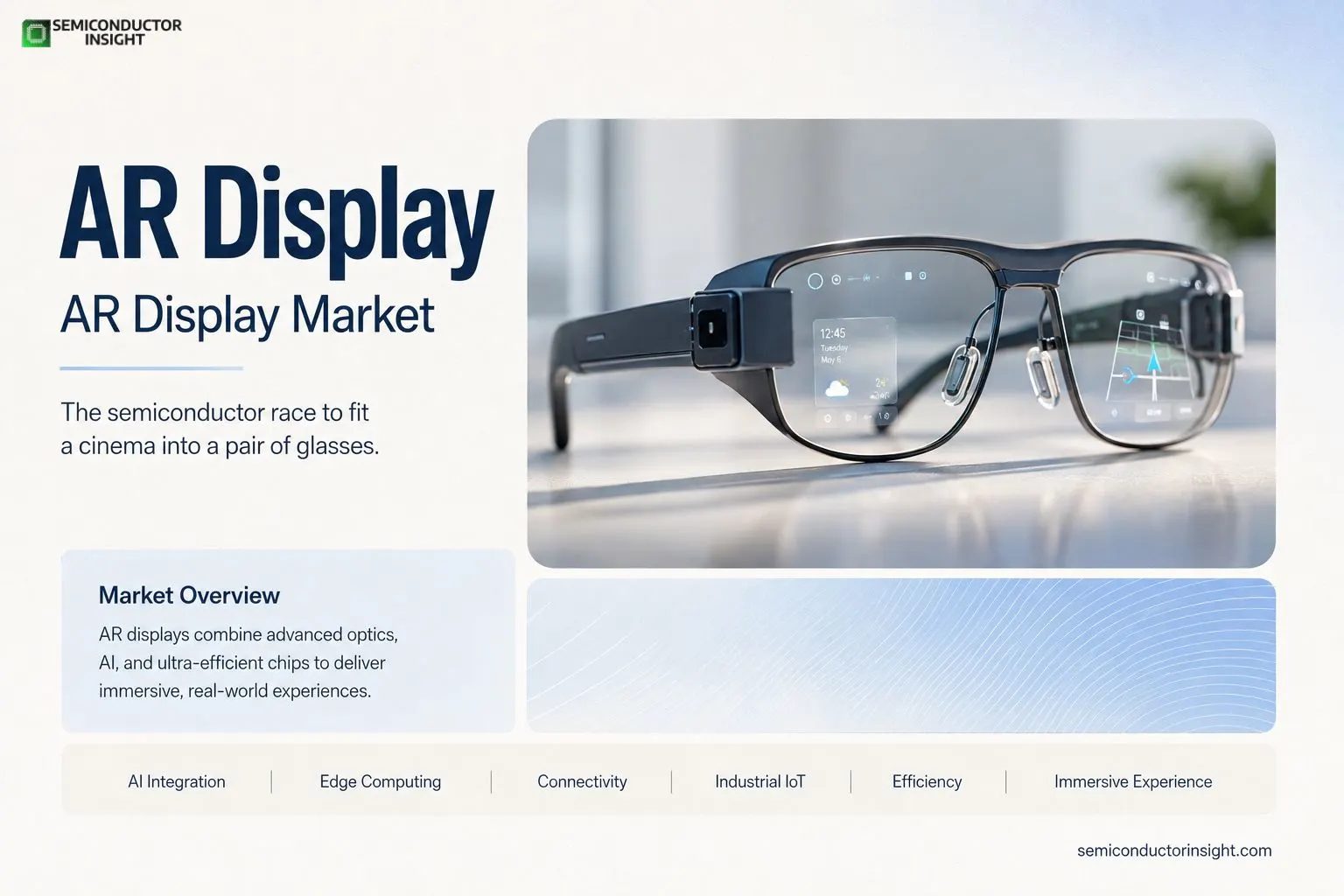
AR Display Market 2026: The Semiconductor Race to Fit a Cinema into a Pair of Glasses
Augmented reality has spent the better part of a decade being the next big thing that always seemed to be just around the corner. Google Glass flickered and faded. Microsoft HoloLens found a home in factories and hospitals but never in living rooms. Magic Leap burned through billions and then quietly pivoted to enterprise. But in 2026, the conversation has shifted. It is no longer about whether someone will crack the AR hardware puzzle. It is about which semiconductor architecture will dominate the solution, because the core challenge of an AR display is, at its heart, a silicon problem.
An AR display is not just a tiny screen. It is a stack of semiconductor-dependent technologies that must work together in a package light enough to sit on a human face for hours. The display engine itself-microLED, microOLED, LCoS, or laser-beam scanning-is fabricated on silicon or compound semiconductor wafers using processes that push lithography to its limits. The waveguide that pipes the image from the display to the eye requires nanoscale gratings etched with the same kind of precision tools used in advanced chip manufacturing. The driver chip that powers the display, the sensor hub that tracks eye movement, the low-latency processor that renders graphics without making the wearer nauseous-all of these are semiconductor devices designed at the most advanced nodes available. In a very real sense, the AR glasses that will eventually replace smartphones are less a consumer electronics product and more a wearable supercomputer wrapped in plastic and titanium.
Why 2026 feels different
Several things have converged this year to make the AR display market feel less like a science project and more like a genuine product category. The first is the maturity of microLED technology. MicroLED displays, which use microscopic gallium nitride or gallium arsenide LEDs as individual pixels, offer brightness and contrast that leave LCD and OLED panels in the dust-critical for outdoor use where AR glasses must compete with sunlight. The challenge has always been manufacturing: bonding millions of microscopic LEDs onto a silicon backplane with near-perfect yield. In early 2026, a major Taiwanese semiconductor foundry, better known for making iPhone processors, confirmed that it had qualified a microLED mass-transfer process for a customer designing AR glasses. The announcement, covered by a leading Asian electronics trade journal, was significant precisely because it was mundane. MicroLED had moved from a research curiosity to a foundry service item, something you could order alongside your chip wafers.
The second is the arrival of purpose-built AR processor chips. Qualcomm’s Snapdragon AR2 platform, first unveiled earlier in the decade, has been iterated into a second generation that splits workloads across a head-worn chiplet and a companion processor in the user’s phone or a tethered compute puck. The headset-bound chip, built on a 4-nanometre process, handles sensor fusion and display driving within a thermal envelope of a few hundred milliwatts-low enough that the glasses do not need a fan. In 2026, at least three major consumer electronics brands are using the platform in products that have either launched or are in carrier trials, a level of ecosystem adoption that makes the AR processor market a genuine semiconductor segment rather than a single-company experiment.
The third is that artificial intelligence finally has a role to play on the device itself. On-device AI accelerators, tiny neural processing units embedded in the display driver or sensor hub, are now capable of running real-time hand tracking, object recognition, and voice command processing without cloud round-trips. This is not a luxury feature; it is a latency requirement. If an AR navigation overlay drifts by even a hundred milliseconds, the user feels queasy. On-device AI solves that problem, but only if the semiconductor can handle the workload within a power budget that does not turn the glasses into a forehead heater.
The waveguide: where optics meets wafer fabrication
While much of the attention goes to the display panel itself, the waveguide is arguably the harder semiconductor-adjacent problem. Waveguides are transparent optical elements-usually made of high-refractive-index glass or polymer-that use diffractive or holographic gratings to steer light from a tiny projector into the user’s field of view. Those gratings are patterned using electron-beam lithography or nanoimprint technology, the same tool families used to make advanced photomasks and semiconductor stamps. The tolerances are brutal: a grating misaligned by a few nanometres can produce a rainbow artefact or dim the image to unusable levels.
In 2026, the waveguide supply chain is still relatively concentrated, with a handful of specialist firms in Europe, the United States, and Japan capable of volume production. But the relationship between these firms and large semiconductor equipment manufacturers is growing closer. Applied Materials and ASML do not build waveguides, but the know-how for nanoscale patterning flows through their customer and partner networks. Several waveguide producers are now using 300-millimetre glass wafers in fabrication lines that look increasingly like semiconductor fabs, complete with cleanroom protocols, automated optical inspection, and statistical process control. When a waveguide factory starts to resemble a chip fab, it signals that the industry is preparing for volumes in the millions, not the thousands.
Where the technology is heading
Looking ahead, the trajectory points toward tighter integration. The display driver, AI accelerator, and image signal processor will merge onto a single chip. The waveguide will become thinner, more efficient, and cheaper as nanoimprint lithography matures. The light engine will shrink to the size of a grain of rice, driven by semiconductor lasers and microLEDs that are essentially tiny pieces of engineered gallium nitride. At that point, the distinction between a display and a semiconductor device becomes meaningless. The display is the semiconductor, and the semiconductor is the display.
The AR display market, for all the consumer hype, is fundamentally a semiconductor story. It is about how far Moore’s Law and its compound semiconductor cousins can push the miniaturisation of light sources, optical elements, and compute logic. In 2026, that story has moved from the preface into the early chapters, and the pace of progress suggests that the long-promised augmented reality, when it finally arrives at scale, will be less a triumph of industrial design and more a victory for the wafer fabs and the patterning tools that make the invisible visible.
Discover the Full Report Now: https://semiconductorinsight.com/report/photonic-integrated-circuits-market/

Comments (0)