

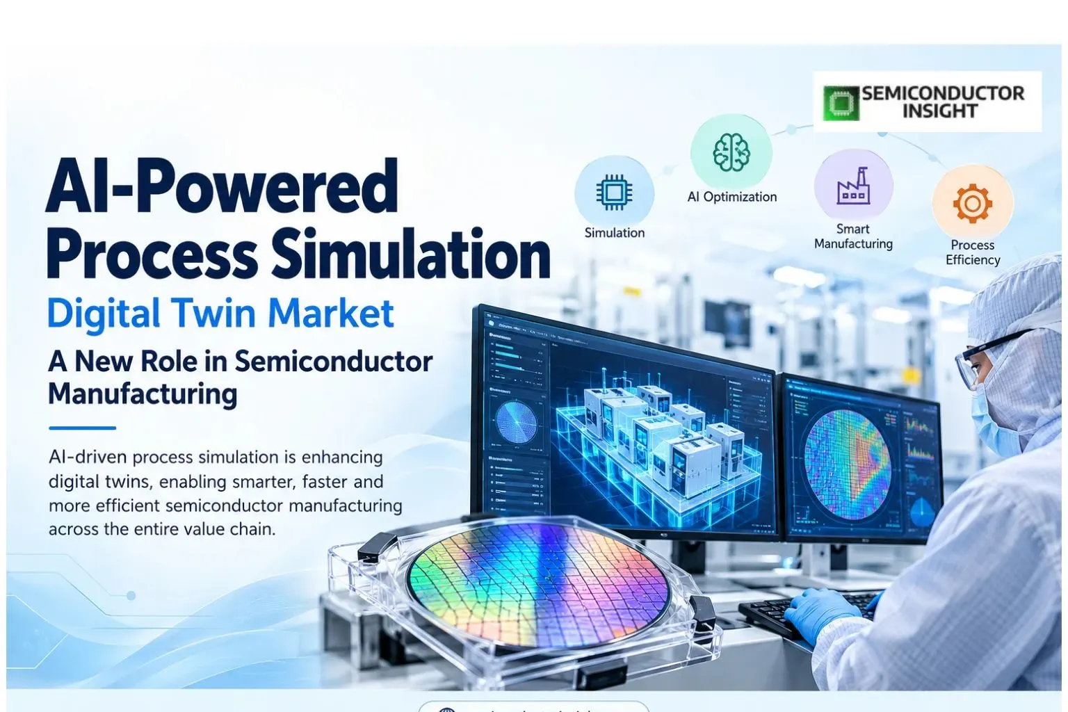
AI-Powered Process Simulation Is Giving Digital Twin Market a New Role in Semiconductor Manufacturing
Semiconductor manufacturing increasingly depends on understanding what happens inside equipment long before a defect appears on a finished wafer. Digital twins help engineers connect physical production assets with virtual models that can simulate process behaviour, evaluate operating conditions, and support decisions using real manufacturing data.
Digital Twin Market is gaining relevance in the semiconductor industry as manufacturers explore AI-assisted process control, virtual fab planning, equipment monitoring, and advanced packaging workflows. Its value lies not simply in creating a 3D factory replica, but in building a useful connection between engineering models and real production operations.
The Virtual Fab Is Becoming an Engineering Tool
- A semiconductor fabrication plant contains interconnected processes involving deposition, lithography, etching, cleaning, inspection, and metrology.
- A change in one operation can affect subsequent stages, making isolated equipment models insufficient for understanding the complete production system.
- A digital twin can combine equipment information, process data, physics-based simulation, and analytical models to examine these relationships.
- Engineers can test hypothetical changes virtually before committing expensive production equipment or risking material during physical trials.
- The distinction matters: a static 3D model represents an asset, while a functional digital twin uses data and models to evaluate its behaviour over time.
A US Semiconductor Initiative Puts Digital Twins on the Manufacturing Agenda
- In January 2025, the US Department of Commerce announced a $285 million award to establish SMART USA, a Manufacturing USA institute focused on semiconductor digital twins.
- The programme was designed to advance digital-twin applications across semiconductor design, fabrication, advanced packaging, assembly, and testing, with a broader planned investment exceeding $1 billion.
The initiative reflects a significant shift in emphasis: digital twins are being considered not only for individual machines but also for interconnected manufacturing processes and the semiconductor supply chain.
For chipmakers, this approach could support virtual process development, equipment integration, and production planning. The intended benefits remain dependent on implementation quality, model validation, and access to reliable operational data.
IIT Madras Brings Digital-Twin Engineering Into Semiconductor Education
An important Indian development emerged on 23 October 2025, when IIT Madras announced an expanded collaboration with Applied Materials India involving the AppliedTwin software framework. The platform is designed to model and optimise semiconductor manufacturing equipment and processes. More than 150 students and faculty members participated in a related hands-on workshop.
This example demonstrates that digital-twin adoption also requires engineering expertise and workforce development. Universities can give students exposure to virtual process modelling before they encounter the complexity of operating fabrication equipment. For India’s semiconductor ecosystem, these capabilities are relevant to manufacturing research, equipment engineering, and advanced packaging.
Foxconn’s Virtual Factory Shows Where AI Changes the Equation
- Electronics manufacturer Foxconn has been developing digital twins of complex production facilities using NVIDIA Omniverse technologies.
- According to NVIDIA’s published case study, AI-assisted computational fluid dynamics simulations for thermal analysis became up to 150 times faster, reducing simulation time from hours to minutes in the described application.
- Although the example concerns electronics manufacturing rather than semiconductor wafer fabrication specifically, it demonstrates how simulation can help evaluate factory airflow, production layouts, robotics, and material movement before physical implementation.
- In semiconductor facilities, similar methods may support cleanroom planning, thermal analysis, equipment placement, and automated material handling.
- These applications are particularly relevant when a facility must accommodate sensitive equipment and tightly controlled environmental conditions.
From Virtual Metrology to Earlier Defect Detection
One emerging application is virtual metrology, in which models estimate process characteristics using available sensor readings and manufacturing data rather than relying exclusively on direct measurements.
A November 2025 report from the US National Institute of Standards and Technology documented semiconductor-industry work exploring shared datasets and AI/ML models for virtual metrology and digital-twin applications. The research examined how data collaboration could improve predictive capabilities across participating organisations.
For semiconductor engineers, the opportunity is to identify process deviations sooner, prioritise physical measurements, and improve production planning. However, these models must be validated against real measurements, particularly where inaccurate predictions could affect yield or device reliability.
Does Tesla Use Silicon Carbide?
Yes. Tesla has used silicon carbide (SiC) power semiconductors in vehicle inverter technology. SiC devices can support efficient power conversion, making them relevant to electric vehicles, charging equipment, and energy systems. Tesla discussed reducing silicon carbide usage by 75% in its next-generation drive unit during its 2023 Investor Day. This was a stated design objective, not a claim that Tesla would eliminate SiC entirely.
The connection to Digital Twin Market is indirect but useful. Digital twins can model power-electronics systems, thermal behaviour, and manufacturing processes involving semiconductor devices. However, Tesla’s SiC use is an example of semiconductor technology adoption, not evidence that Tesla itself uses digital twins for every such process.
To find out more, feel free to browse our latest updated related report: https://semiconductorinsight.com/report/digital-twin-control-market/
What Makes a Semiconductor Digital Twin Trustworthy?
- The US National Institute of Standards and Technology identifies model validation, data management, interoperability, and lifecycle integration as important elements of digital-twin development.
- Its manufacturing research also highlights the need to understand uncertainty and ensure that model results are reliable enough to inform decisions.
- For semiconductor manufacturers, this means a digital twin must be more than an attractive visualisation. It needs dependable sensor data, models that reflect physical behaviour, and a defined method for comparing predictions against actual production outcomes.
As semiconductor processes become more interconnected, digital twins offer a practical way to examine manufacturing decisions before implementing them on the factory floor. Their long-term contribution will depend on how accurately virtual models reflect real equipment, processes, and production constraints.

Comments (0)