

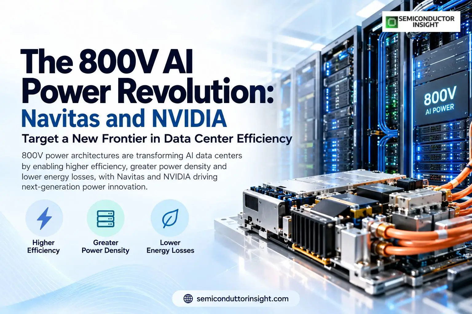
The 800V AI Power Revolution: Navitas and NVIDIA Target a New Frontier in Data Center Efficiency
24kW power delivery. 800V-to-12V conversion. Target efficiency of 97%. A new engineering approach is emerging as AI infrastructure pushes conventional power delivery architectures to their limits.
Against this backdrop, Navitas Semiconductor has unveiled a 24kW, 800V-to-12V DC-DC power delivery board developed in collaboration with NVIDIA, marking another step toward high-voltage DC power architectures for next-generation AI data centers.
Powered by Navitas’ GaNFast gallium nitride (GaN) technology, the new platform is designed to support the NVIDIA MGX ecosystem and address the growing power requirements of advanced AI computing infrastructure. The board is being showcased at the 2026 Open Compute Project (OCP) Global Summit in San Jose, California, taking place from October 12-15.
WHY 800V POWER DELIVERY IS BECOMING A CRITICAL SEMICONDUCTOR INDUSTRY TREND?
AI infrastructure is undergoing a fundamental transformation. As accelerated computing platforms scale, power consumption is rising alongside the need for faster interconnects, more sophisticated cooling, and increasingly compact server architectures.
Traditional power distribution approaches face mounting pressure as systems require higher power within constrained physical footprints. Delivering electricity efficiently from the data center power infrastructure to processors and accelerators is becoming just as important as improving computational performance itself.
High-voltage DC architectures offer a potential pathway to address these challenges by enabling more efficient power distribution and reducing the complexity associated with multiple conversion stages.
For semiconductor manufacturers, this shift creates opportunities across several technology categories, including:
▪Gallium nitride (GaN): High-speed switching capabilities and potential reductions in power-conversion losses and component size.
▪Silicon carbide (SiC): High-voltage power switching technology suited to demanding power conversion and distribution applications.
▪Advanced power packaging: Thermal management and electrical integration approaches that support greater power density.
▪Next-generation power architectures: System designs that bring power conversion closer to processors and accelerators to reduce distribution losses.
Navitas’ latest collaboration with NVIDIA reflects how these technologies are being evaluated at the system level, where semiconductor performance, board design, thermal management, and computing architecture must work together.
- A 24kW power delivery target
The board is designed to deliver 24kW to the compute tray, addressing the substantial electrical demands of modern AI systems. As accelerator platforms become more power-intensive, delivering this level of power within a compact footprint becomes a major engineering consideration.
- Target full-load efficiency of 97%
Navitas specifies a target efficiency of 97% at full load. At this efficiency level, approximately 3% of the input power would be lost during conversion under the stated operating condition.
At 24kW of output, assuming 97% efficiency, the approximate input power would be 24.74kW, with around 742W dissipated as conversion losses. This illustrates why even a small percentage improvement in efficiency can have significant implications for cooling requirements and facility-level energy consumption.
- Power density exceeding 2,000W/in³
The board targets a power density above 2,000 watts per cubic inch, highlighting the importance of delivering substantial power without proportionally increasing the physical dimensions of the power subsystem.
Higher power density can help designers allocate more space to computing hardware, although achieving it also places greater demands on thermal design, component integration, and reliability engineering.
- A compact 400mm × 60mm form factor
Designed around NVIDIA’s specified form factor, the board can be integrated onto the compute motherboard close to the xPUs. This approach is intended to shorten power-delivery paths and reduce losses between the conversion circuitry and the processors or accelerators being powered.
The board incorporates 16 NV6034 GaNFast field-effect transistors, rated at 650V and 18 milliohms, on the primary side. These devices are configured in a stacked half-bridge topology and use Navitas’ dual-cooled DFN 8 × 8 package.
GaN power devices are attracting attention in high-frequency power conversion because their switching characteristics can support compact, high-performance designs when combined with appropriate circuit and thermal engineering.
For AI data centers, this matters because power electronics must operate within increasingly restrictive limits on efficiency, physical size, and heat dissipation.
Navitas’ portfolio also includes GeneSiC silicon carbide technology, positioning the company across two wide-bandgap semiconductor platforms relevant to high-power applications. GaN and SiC serve different device and system requirements, and their relative suitability depends on voltage levels, switching frequency, thermal conditions, and the intended architecture.
The 24kW board therefore represents more than a component-level announcement: it demonstrates how wide-bandgap semiconductor technology can be incorporated into a power subsystem designed around the needs of advanced computing hardware.
FROM 20kW TO 24kW: THE NEXT STEP IN AI POWER SCALING
The new board extends Navitas’ previously announced 20kW, 800V-to-6V power delivery board, also developed in collaboration with NVIDIA.
The two platforms illustrate the importance of architectural flexibility as data center power requirements evolve. Different intermediate-bus voltages and voltage regulator module configurations may suit different processor platforms and point-of-load requirements.
For system designers, the objective is not simply to maximise a single efficiency figure. It is to determine how the entire power chain from incoming electrical infrastructure to the processor can deliver the required current, respond to rapidly changing workloads, and maintain reliable operation.
Navitas has positioned its 800VDC portfolio as a means of giving customers flexibility in selecting intermediate-bus voltages and VRM architectures for their particular applications.
This flexibility could become increasingly valuable as AI infrastructure moves across different accelerator generations, rack configurations, and computing platforms.
WHAT THIS MEANS FOR THE GLOBAL SEMICONDUCTOR INDUSTRY
The collaboration highlights several developing opportunities across the semiconductor and data center supply chains.
Power semiconductors are becoming strategic AI infrastructure components. As computing demand increases, the performance of power conversion systems can directly influence energy efficiency, thermal management, and the practical deployment of high-density computing hardware.
Wide-bandgap devices are gaining relevance beyond traditional industrial applications. GaN and SiC technologies are increasingly being considered for power conversion challenges where switching performance, efficiency, and system density are important design priorities.
Power architecture is becoming a competitive differentiator. Semiconductor suppliers will increasingly need to demonstrate how their devices perform within complete power delivery systems, rather than relying solely on individual component specifications.
Collaboration between chip suppliers and computing platform developers is becoming more consequential. Joint engineering can align power electronics with the electrical, mechanical, and thermal requirements of next-generation compute platforms.
At the same time, the commercial impact of 800VDC adoption will depend on broader ecosystem readiness, including compatible power infrastructure, safety standards, protection systems, manufacturing scalability, and integration across data center designs.
Get Instant Access to Our Latest Research Highlights: https://semiconductorinsight.com/report/global-power-semiconductors-market/

Comments (0)