
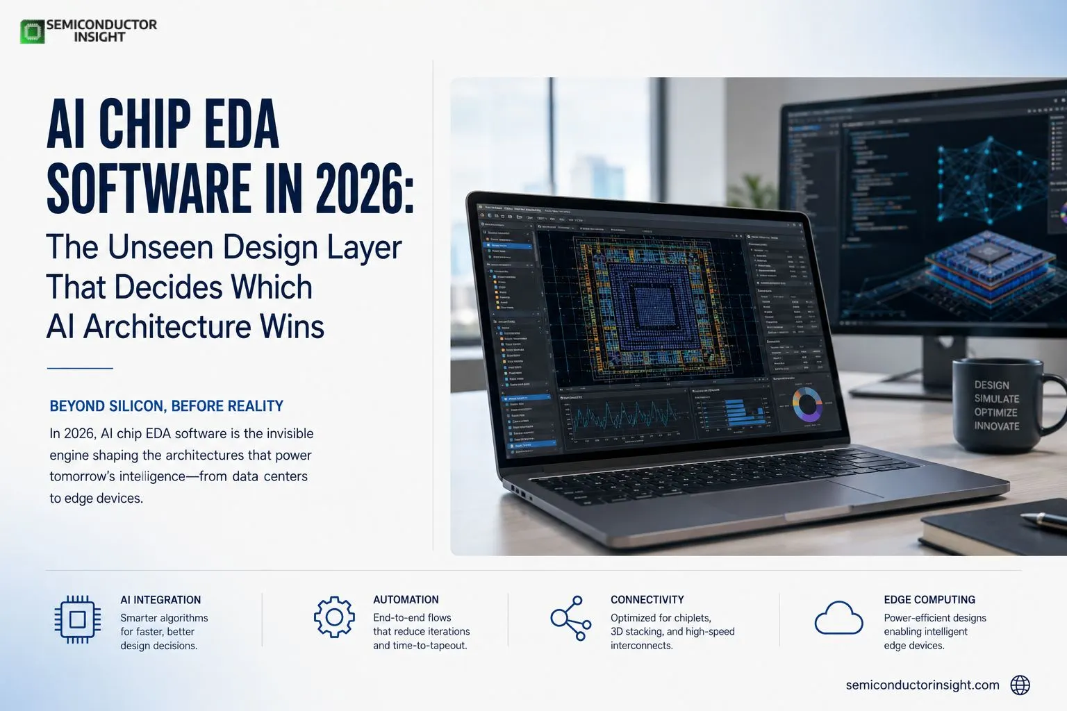
AI Chip EDA Software in 2026: The Unseen Design Layer That Decides Which AI Architecture Wins
Before a single square millimetre of silicon is taped out, before the photomasks are made, before the billion-dollar fab even knows the chip exists, something quieter and arguably more decisive has already happened. The architects of an AI acceleratorwhether it is destined for a hyperscale data centre or a tiny embedded sensorhave spent months inside a virtual world. They have moved logic blocks across a screen, balanced power grids, run endless simulations of thermal hotspots, and watched simulated neural networks fire across imaginary circuits. The software that makes this possible is called electronic design automation, and in 2026, the subset of it built specifically for artificial intelligence chips has become one of the most strategic, and least visible, layers of the semiconductor industry.
AI chip EDA software is not the same as the general-purpose tools that laid out the CPUs of the 1990s or the smartphone SoCs of the 2010s. It is a category of specialised platforms that integrate circuit synthesis, floorplanning, power analysis, andincreasinglymachine-learning-driven optimisation into a single flow. Their purpose is to help engineers design chips whose architectures are themselves shaped by AI: massive arrays of multiply-accumulate units, memory-on-logic stacks, chiplet-based systems, and dataflow engines that look nothing like a traditional processor core. If a conventional EDA tool is a Swiss Army knife, an AI chip EDA suite is a surgeon’s scalpel, honed for one patient.
Why AI chips broke the old EDA model
Traditional EDA tools were built for a world where a chip was a fairly predictable assembly of processor cores, cache, and I/O. They could handle incremental improvements in clock speed and gate count. But an AI acceleratorthink of the tensor cores inside an NVIDIA GPU, or the systolic arrays in a Google TPU, or the custom silicon that Amazon trains its recommendation models onis an entirely different beast. These chips are dominated by repetitive arrays of simple compute elements. Their performance is bound not just by transistor speed but by memory bandwidth, data movement energy, and the delicate balance between parallelism and latency. Floorplanning an AI chip is more like solving a city-planning problem where the roads carry terabytes of traffic every second and a single traffic jam kills performance.
In 2026, the complexity has ratcheted up again. AI models are no longer just large; they are structurally varied. One week a startup wants to run a sparse mixture-of-experts transformer, the next week a hyperscaler is designing a chip for diffusion models that generate video. EDA tools must now allow architects to explore radically different dataflow schemes, to simulate how a design will perform on a workload that does not yet exist in silicon, and to co-optimise the chip hardware and the compiler that will map software onto it. This is a feedback loop that generic EDA was never designed to close.
The AI tool that designs AI chips
One of the most interesting developments in 2026 is that AI is being used to design AI chips. It has a recursive elegance that is not lost on the engineers doing it. Reinforcement learning agents, trained on vast libraries of past designs, can now suggest optimal floorplans, power grid placements, and clock tree routing in a fraction of the time a human team would need. In February 2026, at a technical conference covered by a leading semiconductor engineering trade journal, a major EDA vendor demonstrated a tool that used a graph neural network to predict routing congestion in a 3‑nanometer AI accelerator design before a single wire was drawn. The prediction was accurate enough that the design team eliminated three weeks of manual iterations, helping the chip tape out ahead of schedule. These are not academic curiosities; they are being deployed inside the world’s most advanced chip design houses.
The adoption of AI-driven optimisation inside EDA has a straightforward economic motive. A single respin of a leading-edge chipcorrecting a flaw found after manufacturingcan cost tens of millions of dollars and push a product launch back by six months. In the AI chip race, where a new accelerator can be obsolete in two years, that delay can be fatal. EDA tools that catch problems early, or that shrink the design cycle, pay for themselves on the first project. As a result, the R&D budgets of Synopsys, Cadence, and smaller specialised firms are flowing heavily into AI-assisted design, and the AI chip EDA segmentwhile still a fraction of the broader EDA marketis growing at a rate that significantly outpaces the rest.
The open-source undercurrent
Not everything in AI chip EDA happens behind the paywalls of commercial tool vendors. A grass-roots movement built around open-source hardware designanalogous to what Linux did for operating systemsis gaining traction. Projects like OpenROAD and the CHIPS Alliance offer no-cost digital design flows that can take a chip from RTL to GDSII. While they are not yet competitive with commercial tools at the bleeding edge, they are proving increasingly capable for mid-range nodes and research chips. Several university teams and government-backed research institutes used open-source EDA flows to tape out AI accelerators in 2025 and early 2026, according to reports in specialist electronics media. This democratisation could eventually reshape the market, making it possible for smaller companies to design custom AI silicon without an eight-figure EDA licence fee.
A 2026 signal from the foundry ecosystem
The interplay between EDA tools and the foundries that manufacture chips is another critical piece of the puzzle. In March 2026, a major semiconductor foundry announced a design-technology co-optimisation partnership with a leading EDA vendor specifically for AI accelerator chiplets. The collaboration, reported by a reputable industry publication, was aimed at enabling designers to work with the foundry’s advanced 3‑nanometre process and its 3D stacking technology within a single unified EDA environment. The announcement matters because it shows that EDA tools are no longer just a design aid; they are becoming a competitive differentiator for foundries themselves. When TSMC, Samsung, or Intel Foundry wants to attract AI chip customers, the quality and integration of the EDA toolchain they can offer becomes part of the pitch.
The chiplet effect and the disaggregation of design
The shift toward chiplet-based architectureswhere an AI accelerator is built from multiple smaller dies stitched togetherhas added another layer of complexity. A chiplet design must manage inter-die communication, thermal cross-talk, and signal integrity across a silicon interposer or organic substrate. Traditional EDA flows treat a chip as a monolithic entity; AI chip EDA software in 2026 is being forced to evolve into a multi-die, system-level design environment. This is not a trivial extension. It requires the tool to simultaneously optimise placement across multiple dies, to co-simulate power delivery networks that span packages, and to verify that the interfaces between chiplets from different process nodes will work reliably. The companies that solve this problem will own the next decade of EDA for high-performance computing.
The human element that software cannot replace
For all the automation and AI assistance, the design of an AI chip remains a deeply human art. The EDA tool can suggest a thousand floorplan variations, but a senior architect must know which ones make sense for the specific model the chip will run. It can simulate power at every corner case, but an engineer who has seen a chip burn up on a test bench knows something that a thermal map cannot capture. The best AI chip EDA platforms are not trying to replace these instincts; they are trying to amplify them, to give the architect more cycles to think about architecture rather than fighting tool glitches. In 2026, the most productive design teams are the ones that have learned to blend algorithmic optimisation with hard-won experience, and the EDA vendors that support that blend are winning the long-term loyalty of their customers.
As the year unfolds, AI chip EDA software continues its quiet, essential work behind the scenes. It does not generate the excitement of a new large language model or a record-breaking GPU benchmark. But without it, none of those things would exist. It is the invisible scaffolding that supports the cathedral of AI silicon, and as the cathedral grows taller and more complex, the scaffolding must grow stronger, smarter, and more adaptable. The tools that shape the chips are, in their own way, shaping the future of intelligence itself.
Read our new report quick and valuable: https://semiconductorinsight.com/report/ai-chip-eda-software-market/

Comments (0)