

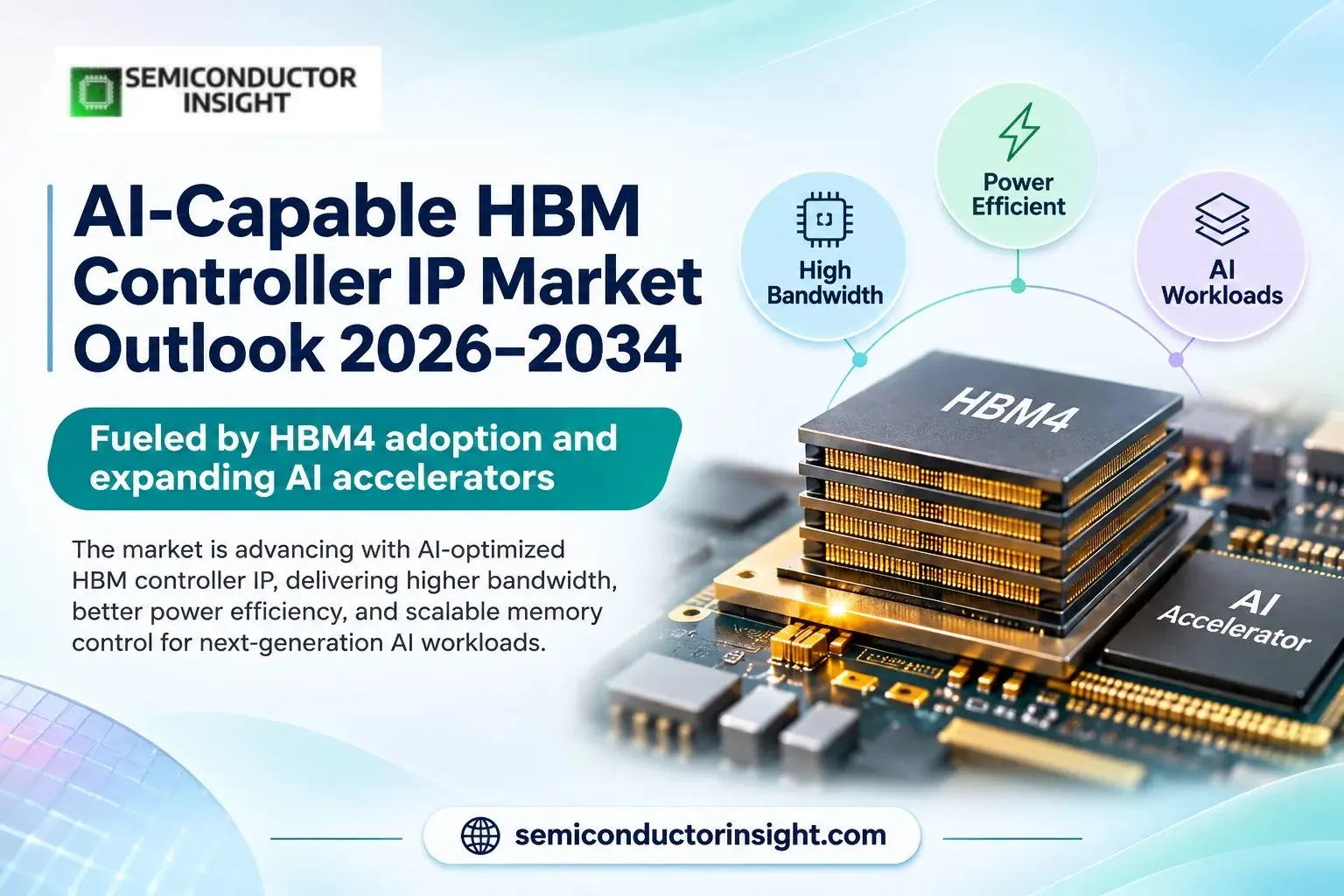
AI-Capable HBM Controller IP Market Outlook 2026-2034 amid HBM4 Adoption and AI Accelerator Expansion
The growing complexity of artificial intelligence workloads is changing how semiconductor designers approach memory architecture. Large language models, generative AI, recommendation engines, and high-performance computing applications require processors to retrieve and process enormous volumes of data without creating bottlenecks around memory access. High Bandwidth Memory (HBM) has become central to this requirement, but increasing memory capacity alone is not enough. The controller responsible for scheduling, coordinating, and optimizing data movement is becoming equally important.
The AI-Capable HBM Controller IP Market is gaining relevance as chip developers look for reliable, low-latency, and power-efficient memory subsystems capable of supporting increasingly demanding accelerator architectures. The shift toward custom AI silicon is also creating opportunities for specialized IP that can be integrated into ASICs, GPUs, and next-generation computing platforms.
The HBM4 Architecture Is Rewriting Controller Design
The transition from HBM3E to HBM4 represents more than a routine memory upgrade. HBM4 introduces a 2,048-bit interface compared with the 1,024-bit interface used in HBM3E, alongside an expansion from 16 to 32 channels. This wider architecture increases the amount of data that can move between memory and processors, but also places greater demands on controller logic, interface timing, interconnect design, and system-level coordination.
Controller IP developers are adapting to these requirements through advanced scheduling mechanisms, optimized command handling, channel management, memory access prioritization, and improved subsystem integration. The architectural shift is creating a new design cycle for semiconductor companies transitioning toward HBM4-based AI accelerators.
AI Chipmakers Are Moving Toward Faster Memory Subsystems
AI accelerator performance increasingly depends on how efficiently data reaches compute units rather than simply how many processing cores a chip contains. Memory bandwidth, latency, data availability, and energy consumption directly influence workload execution, especially in large-scale model training and inference.
In March 2026, Rambus announced its HBM4E Controller IP supporting data rates of up to 16 Gbps per pin. GUC also announced its HBM4E PHY and Controller IP in September 2026, targeting 16 Gbps operation using TSMC’s N2P process. These developments demonstrate how memory interface IP suppliers are preparing for higher-bandwidth AI architectures and more advanced chip integration requirements.
Why Controller IP Is Becoming a Chip-Level Design Priority?
The controller is no longer treated as an isolated memory interface component. Its performance directly influences how efficiently accelerator cores, memory stacks, interconnects, and power-management systems operate together.
Modern HBM controller solutions increasingly incorporate features such as error management, memory scheduling, pseudo-channel operation, performance monitoring, configurable interfaces, and reliability-related mechanisms. Designers are also focusing on minimizing power consumption during intensive memory traffic, particularly for AI systems deployed across large data-center clusters where energy efficiency influences operating costs.
This makes controller IP selection a critical decision during the early stages of custom ASIC development rather than a late-stage integration activity.
Advanced Packaging Is Changing the IP Integration Equation
HBM stacks are increasingly integrated alongside compute dies through advanced packaging technologies such as silicon interposers and 2.5D or 3D architectures. These arrangements shorten interconnect distances and support wider memory interfaces, but they introduce demanding signal-integrity, power-integrity, thermal, and physical-design considerations.
GUC’s April 2026 HBM4 demonstration combined its controller and PHY with TSMC’s 3nm technology and CoWoS packaging. Its September HBM4E announcement further highlighted compatibility with advanced 3D integration concepts. These developments show how controller IP is increasingly developed alongside packaging architecture, process-node selection, and physical implementation rather than independently.
Stay connected for additional in-depth information right here: https://semiconductorinsight.com/report/ai-capable-hbm-controller-ip-market/
Verification Is Moving Closer to the Product Development Cycle
At higher data rates, successful IP integration depends on more than protocol compliance. Engineers must validate timing behavior, initialization, memory training, error handling, channel operation, and system performance under different workload conditions. Verification environments involving memory models, test benches, emulation, and post-silicon monitoring are becoming increasingly important.
For HBM4 architectures, 32 independent channels and a 2,048-bit data interface create a much wider validation landscape than previous memory generations. Early verification and integration support can help semiconductor developers identify problems before expensive advanced-node fabrication and packaging stages.
Where the Next Design Wins May Emerge
The expanding ecosystem of AI accelerators, custom cloud processors, networking ASICs, HPC systems, and specialized inference chips is creating a broader application base for high-performance memory controller IP. Companies developing custom silicon are increasingly evaluating memory IP alongside compute architecture, foundry compatibility, packaging availability, and long-term performance scaling.
The next competitive advantage may not come simply from supporting the fastest memory data rate. It will increasingly depend on how well controller IP combines bandwidth, power efficiency, reliability, verification readiness, and compatibility with advanced chip architectures.
The AI-Capable HBM Controller IP Market is therefore becoming an important part of the wider AI semiconductor ecosystem, with the HBM4 and HBM4E transition opening new design opportunities for memory-interface specialists and custom-chip developers worldwide.

Comments (0)