
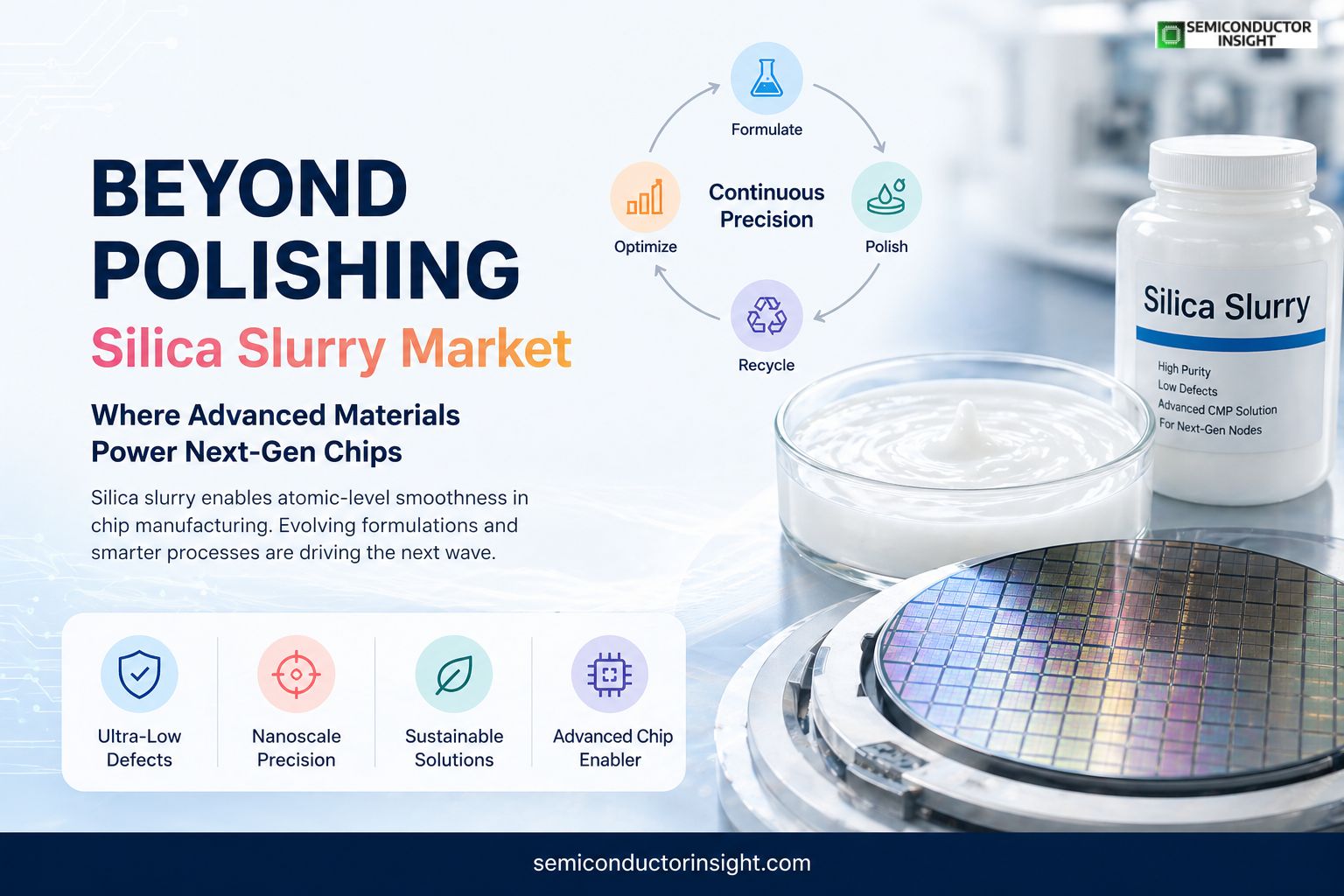
Advanced Materials Evolution within Silica Slurry Market for Modern Chips
Silica slurry has become essential in the worldwide semiconductor sector, where performance is determined by nanometre-scale precision. Silica slurry, which is typically used in chemical mechanical planarization (CMP), guarantees extremely flat wafer surfaces, making it possible to stack intricate integrated circuits.
As chipmakers push toward 3 nm and even sub-2 nm nodes, the tolerance for surface variation has narrowed to less than 1 nanometre, making slurry formulation a critical enabler rather than just a consumable.
Silica slurry typically consists of colloidal silicon dioxide particles suspended in a chemically active solution. These particles, often sized between 20 nm and 100 nm, act as abrasive agents during polishing.
A single 300 mm wafer may require approximately 2 to 5 liters of slurry during multiple CMP steps, depending on process complexity. With over 7 million 300 mm wafers processed globally per month as of 2025, slurry consumption volumes have scaled significantly, crossing an estimated 250 million liters annually across fabs worldwide.
Where Material Science Meets Chip Complexity?
The size of the particles is not the only thing that sets modern silica slurry apart from prior versions. The homogeneity and chemical stability of the particles are also important. Semiconductor makers now want defect densities to be less than 0.01 faults per square centimeter. This forces slurry makers to improve their impurity management and dispersion methods. Even tiny amounts of metals that are less than 10 parts per billion can affect the yield of modern logic and memory devices.
The focus of recent developments has been on slurry formulae that are tailored for specific layers:
- Polishing copper interconnects that need to remove 100-300 nm per minute at a controlled rate
- Planarization of the dielectric layer that needs ultra-low dishing < 5 nm
- Tungsten CMP methods that keep selectivity ratios exceeding 50:1
- This level of accuracy is necessary because current processors can have more than 100 billion transistors, and each one needs perfect stacking.
Review the latest market intelligence in the complete related report: https://semiconductorinsight.com/report/cmp-silica-slurry-market/
Scaling Demand with Semiconductor Expansion
The expansion of semiconductor fabrication facilities globally is directly influencing silica slurry demand. A leading-edge fab can consume between 5,000 to 10,000 litres of slurry per day. With more than 80 new fabs announced or under construction worldwide between 2023 and 2026, the cumulative demand is accelerating.
Memory manufacturing alone contributes significantly. A typical DRAM wafer undergoes 20 to 30 CMP steps, while NAND flash production may involve over 40 polishing stages. This translates into higher slurry intensity per wafer compared to logic chips. In volume terms, memory fabs account for nearly 45% of total slurry consumption globally.
Meanwhile, the shift toward heterogeneous integration and advanced packaging has introduced additional CMP steps at the packaging level, further extending slurry usage beyond front-end processes.
The Quiet Evolution behind AI and High-Performance Computing
- The rise of artificial intelligence and high-performance computing has indirectly elevated the importance of silica slurry.
- GPUs and AI accelerators rely on advanced nodes and multi-layer interconnects, both of which require highly controlled planarization.
For instance, a single advanced AI chip may involve over 1,000 individual process steps, with CMP contributing to nearly 10-15% of total fabrication stages. Without effective slurry performance, issues like erosion, dishing, or micro-scratches could compromise signal integrity and thermal efficiency.
- Notably, leading semiconductor manufacturers have recently adopted slurry recycling systems, recovering up to 60-70% of used slurry volume.
- This not only reduces operational costs but also addresses environmental concerns, as slurry waste can exceed 1,000 litres per fab per day.
Beyond Polishing a Strategic Material in Focus
Silica slurry is increasingly being viewed as a strategic material rather than a commodity. Its formulation impacts yield, throughput, and ultimately the cost per wafer. A 1% improvement in yield at advanced nodes can translate into millions of dollars in annual savings for a single fab.
Emerging trends include:
- Development of ultra-low particle size distributions below 10 nm for next-gen nodes
- Integration of AI-driven monitoring systems to optimize slurry usage in real time
- Shift toward environmentally benign chemistries with reduced pH variability
- Customization of slurry for compound semiconductors like silicon carbide and gallium nitride
- These innovations reflect a broader transformation where materials science is tightly integrated with semiconductor engineering.
A Subtle yet Powerful Force in Chip Manufacturing
While often overlooked compared to lithography or etching technologies, silica slurry plays a foundational role in enabling the semiconductor ecosystem. Its evolution mirrors the industry’s relentless pursuit of precision, efficiency, and scalability. As chips continue to shrink and architectures grow more complex, the importance of achieving atomic-level smoothness will only intensify.
In many ways, Silica Slurry Market is not just supporting semiconductor growth it is quietly defining its limits.

Comments (0)