
Advanced Innovation Trends in Chip Package Test Probes Market
In today’s semiconductor ecosystem, chip package test probes play a silent yet critical role in ensuring device reliability. These probes create temporary electrical connections between testing systems and packaged chips, validating performance before final deployment. As chip architectures become increasingly complex, the importance of precision testing has intensified across industries like consumer electronics, automotive, and telecom.
The evolution of packaging technologies such as BGA, CSP, and system-in-package has significantly increased the demand for advanced probing solutions. In fact, nearly 62% of semiconductor applications rely on probe-based validation across logic, memory, and system-on-chip devices.
For instance, in January 2026, India has established an anti-dumping investigation against imports of nylon granules and chips from China and Russia, which are vital parts of the textile sector. The investigation was started by the trade ministry’s Directorate General of Trade Remedies (DGTR) in response to a complaint made by a domestic manufacturer.
Rising Complexity Driving Market Momentum
The Chip Package Test Probes Market is expanding due to rapid advancements in semiconductor design and manufacturing. The shift toward smaller nodes and higher I/O density has pushed manufacturers to adopt high-density probing solutions capable of handling intricate chip layouts.
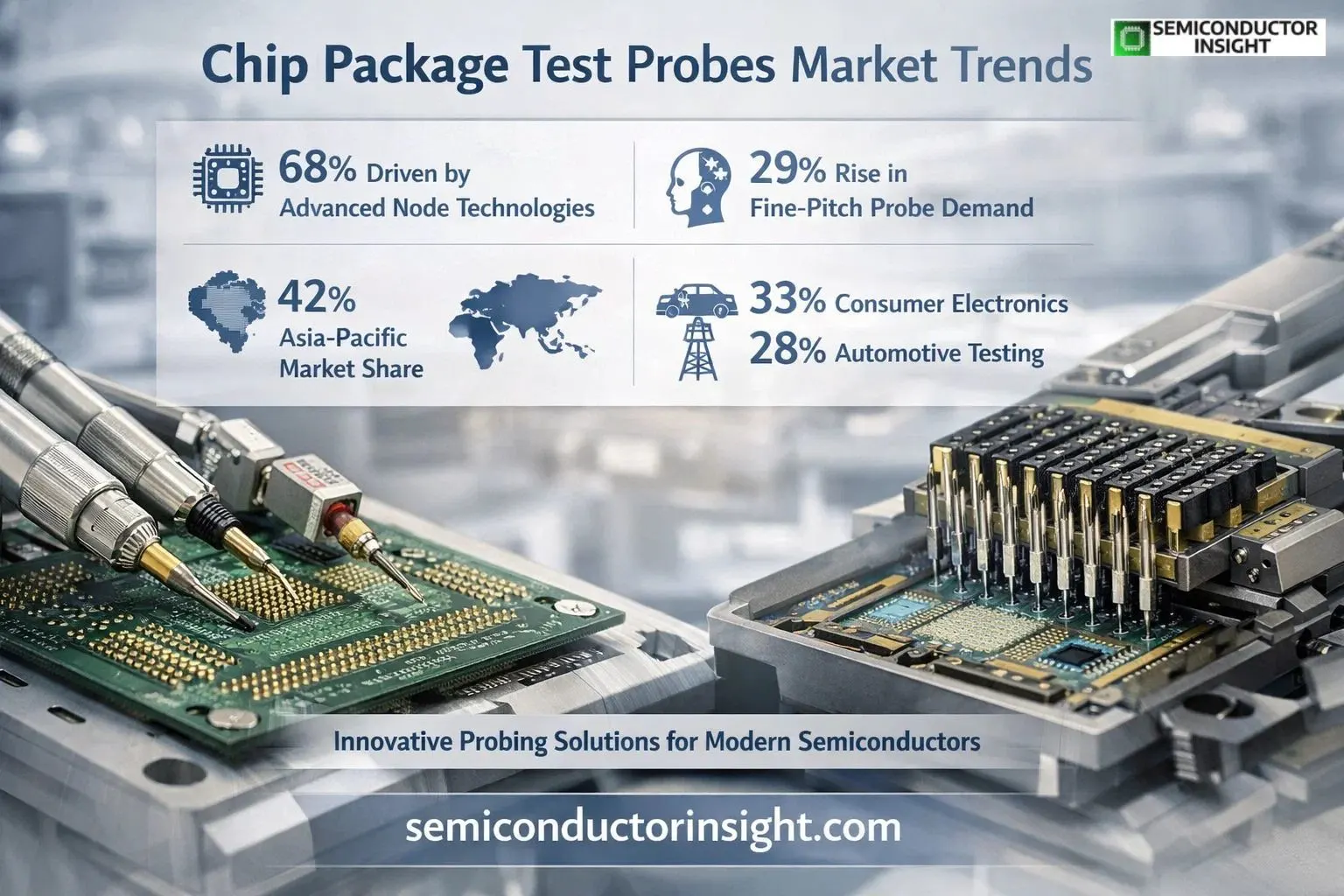
Over 68% of testing demand is now influenced by advanced node technologies, while approximately 73% of probe usage is linked to increasing packaging complexity.
Additionally, the surge in AI processors and IoT-enabled devices has resulted in a 29% rise in demand for fine-pitch probes, reflecting the need for ultra-precise contact testing in compact chip designs.
Technology Evolution Shaping the Industry
· Innovation remains at the core of this market, with manufacturers focusing on improving durability, signal accuracy, and testing efficiency. Modern probe solutions now integrate MEMS technology, enabling better alignment and repeatability.
· MEMS-based probe cards alone account for nearly 48% of total probe card adoption, highlighting their dominance in high-performance testing environments.
· Furthermore, around 36% of new product developments are centred on ultra-fine pitch probing systems, while 28% integrate combined thermal and electrical testing capabilities, reducing overall testing cycles.
· These advancements are enabling faster validation processes, especially for high-frequency and high-speed semiconductor applications.
Regional Production and Demand Landscape
Asia-Pacific continues to dominate the Chip Package Test Probes Market, accounting for approximately 42% of global share, driven by strong semiconductor manufacturing hubs in China, Japan, and South Korea.
The region’s leadership is further supported by large-scale production volumes, with over 700 million probe units manufactured annually, reflecting the massive scale of semiconductor testing operations.
Meanwhile, North America contributes significantly through innovation and R&D, with increasing adoption of advanced probe systems in AI and automotive chip testing. Europe also maintains steady demand, particularly in industrial and automotive electronics.
To find out more, feel free to browse our latest updated report: https://semiconductorinsight.com/report/global-chip-package-test-probes-market/
Industry Wide Adoption and Market Penetration
· The use of chip package test probes extends across multiple industries, with consumer electronics accounting for nearly 33% of total usage, followed by automotive at 28%, and telecommunications at 21%.
· The automotive sector, in particular, is witnessing rapid growth due to the integration of advanced driver-assistance systems (ADAS) and electric vehicle technologies. These applications demand highly reliable semiconductor components, further increasing the need for robust testing solutions.
· Additionally, the rise of 5G infrastructure has led to a 22% increase in high-frequency chip testing, emphasizing the importance of accurate and efficient probe technologies.
· Challenges and Future Outlook
· Despite strong growth, the market faces challenges such as probe wear and tear, with failure rates increasing by over 10% in complex multi-chip environments.
· However, the future remains promising as innovations in hybrid probe designs and AI-assisted diagnostics continue to improve testing accuracy and efficiency. The integration of automated inspection systems, now adopted in over 30% of new testing setups, is expected to further enhance productivity and reduce downtime.
Chip Package Test Probes Market stands as a foundational pillar in semiconductor manufacturing, ensuring that increasingly complex chips meet performance and reliability standards. With growing demand from AI, automotive, and high-speed communication technologies, the market is set to witness sustained innovation and expansion.
As semiconductor devices continue to shrink while performance expectations rise, the role of precision testing solutions will only become more vital making chip package test probes indispensable to the future of electronics.

Comments (0)