ABF Substrate Market Outlook as Advanced Packaging Becomes the New Battleground
The semiconductor industry is entering a phase where performance gains are no longer delivered by transistor scaling alone. As chips grow more complex and workloads demand higher data throughput, the importance of advanced packaging materials has moved sharply into focus. At the centre of this transition lies the ABF substrate, a foundational component that quietly determines how effectively a chip communicates with the outside world.
Once considered a specialized input, ABF substrates are now strategic assets. Their availability, performance, and manufacturing precision directly influence the success of high-end processors used in data centers, artificial intelligence, high-performance computing, and next-generation networking infrastructure.
Before Scrolling, Surf Our Latest Report for More Detailed Insights:
https://semiconductorinsight.com/report/abf-substrate-market/
From Interconnect Material to Industry Bottleneck
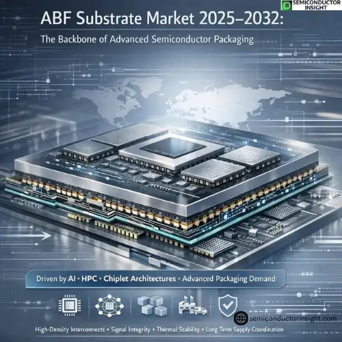
ABF substrates are epoxy-based build-up films used to create ultra-fine wiring layers in semiconductor packages. Their key role is enabling high-density signal routing between the silicon die and the system board. As chip architectures have evolved toward higher I/O counts and tighter spacing, traditional substrate technologies have struggled to keep pace.
This has elevated ABF from a supporting material to a potential bottleneck. In recent years, demand has consistently outpaced supply, particularly for high-layer-count substrates required in advanced logic devices. This imbalance has reshaped procurement strategies and driven long-term capacity planning across the semiconductor value chain.
Packaging Complexity Is Redefining Substrate Requirements
- Modern chips are no longer simple monolithic structures. Advanced processors increasingly rely on chiplets, heterogeneous integration, and multi-die configurations. These architectures place enormous demands on the substrate’s electrical performance, thermal stability, and dimensional accuracy.
- ABF substrates are being engineered with finer line widths, improved dielectric properties, and enhanced thermal resistance to meet these challenges. Even minor deviations in substrate quality can impact signal integrity or yield, making consistency as critical as innovation.
- As a result, substrate development timelines are now closely aligned with processor roadmaps, rather than trailing them.
AI and HPC Are Reshaping Demand Patterns
The rapid rise of AI acceleration and high-performance computing has fundamentally altered ABF substrate demand. These applications require large packages with high pin counts, multiple layers, and exceptional reliability under sustained thermal loads.
Unlike consumer electronics, where cost sensitivity dominates, AI and HPC prioritize performance and uptime. This has shifted ABF substrate market toward premium products with higher margins and longer qualification cycles.
Manufacturers are responding by focusing on specialized formulations and process optimization rather than broad commoditization.
Capacity Expansion Comes with Structural Constraints
- While substrate suppliers are expanding capacity, ABF manufacturing is capital-intensive and technically demanding.
- New production lines require years of planning, significant investment, and deep process expertise.
- Yield ramp-up is gradual, and full utilization often lags installation by several quarters.
- These constraints mean supply growth remains disciplined rather than aggressive.
- For chipmakers, this reinforces the importance of long-term supply agreements and early engagement with substrate vendors.
- The market is therefore characterized not by short-term volatility, but by structural tightness that rewards strategic coordination.
Geographic Concentration Shapes Market Dynamics
ABF substrate production is highly concentrated in East Asia, where ecosystem maturity, skilled labor, and proximity to advanced packaging facilities provide competitive advantages. This regional concentration has introduced geopolitical and logistical considerations into what was once a purely technical market.
In response, semiconductor companies are reassessing sourcing strategies and exploring diversification, although replicating ABF manufacturing expertise outside established hubs remains challenging.
Rather than rapid relocation, the market is likely to see incremental geographic balancing over time.
Technology Collaboration Is Becoming the Norm
The ABF substrate market is no longer driven by off-the-shelf solutions. Chip designers, OSATs, and substrate manufacturers are increasingly working together during early development stages. This collaboration helps align substrate capabilities with package architecture, power delivery requirements, and signal routing needs.
Such integration reduces late-stage redesign risks and accelerates time to market. It also raises entry barriers, as new suppliers must demonstrate not only manufacturing capability but also deep technical alignment with customer processes.
Cost Pressures without Compromising Reliability
- Although performance remains the top priority, cost management has not disappeared from the equation. Substrate manufacturers are under pressure to improve yields, reduce material waste, and optimize layer stacking efficiency.
- However, cost reduction in this market is evolutionary rather than disruptive. Reliability failures in high-end processors carry consequences far greater than marginal savings, ensuring that quality remains non-negotiable.
- This balance reinforces the ABF substrate market’s reputation as a precision-driven, trust-based segment.
Market Trajectory: Strategic Growth with Long Visibility
The ABF substrate market is positioned for sustained growth, supported by long semiconductor investment cycles and expanding advanced packaging adoption. Unlike short-lived technology trends, the drivers behind ABF demand data intensity, compute density, and architectural complexity are structural.
Growth will be paced, capacity additions will be deliberate, and competition will favor expertise over scale alone.
Wrapping Up
ABF substrate market exemplifies how seemingly invisible materials can shape the future of computing. As semiconductor innovation shifts from transistor scaling to system-level optimization, substrates have become critical enablers rather than passive components.
In the years ahead, success in advanced chips will depend as much on packaging precision as on silicon brilliance and ABF substrates will remain at the centre of that equation.
Comments (0)