Key Statistics
Key Takeaways
- 4–8 Layers ABF Substrate is the leading type on the source page with a stated 69% share, reflecting the large installed base of mainstream CPU, PC and general computing packages where cost, yield and interconnect density remain balanced.
- PCs are identified as the largest application with a stated 40% share, but Server & Data Center and HPC/AI Chips are the strongest structural growth areas because AI packages are becoming larger, more layered and more routing-intensive.
- China Taiwan is identified on the source page as the largest market with a 30% share, followed by China mainland and South Korea at 17% each; this geography is consistent with the concentration of advanced packaging and substrate manufacturing in East Asia.
- The market is highly concentrated. The source page states that Unimicron, Ibiden, AT&S, Nan Ya PCB and Shinko Electric Industries together hold about 74% of the market, making qualified capacity and customer relationships important barriers to entry.
- Current supplier investment confirms AI-driven demand. Ibiden announced approximately ¥500 billion of high-performance IC package-substrate investment for FY2026–FY2028, while AT&S announced a €1.5–2.0 billion Kulim expansion tied to long-term customer commitments.
ABF Substrate Market Overview
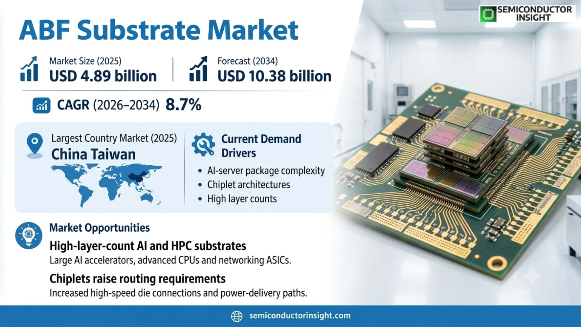
ABF substrate market is rebased to USD 4.89 billion in 2025, increases to an estimated USD 5.32 billion in 2026, and is projected to reach USD 10.38 billion by 2034. The selected source-page size anchors imply a 8.7% CAGR during 2026–2034. China Taiwan is the largest country market in 2025, while current demand is being reshaped by AI-server package complexity, larger chip packages, chiplet architectures, higher layer counts and the rapid buildout of qualified IC-substrate capacity across Japan, Taiwan, Korea, China and Malaysia.
ABF substrates are advanced organic IC package substrates that use Ajinomoto Build-up Film as an interlayer insulating material around fine copper circuitry. The material enables thin dielectric layers, fine vias and dense redistribution between a semiconductor die and the printed circuit board. Commercial performance depends not only on the ABF resin itself but also on line-and-space control, laser-via accuracy, warpage management, copper adhesion, surface treatment and multi-layer yield.
The demand mechanism is changing as AI accelerators, high-end CPUs and chiplet-based packages become physically larger and electrically more complex. Ibiden reported in 2025 that the production load of AI-server substrates could reach roughly 1.8 times its 2024 level in 2026 and 2.5 times by 2027, while AT&S said in 2026 that the shift from monolithic chips toward chiplet-based and heterogeneous architectures is increasing demand for larger, more advanced substrate solutions.
Supply expansion is therefore moving in parallel with technology migration. Ibiden’s Ono Plant began mass production for AI-server and networking package substrates in 2025, and the company approved a further multi-year investment program in 2026. AT&S is ramping its Kulim, Malaysia site and plans further expansion with customer commitments. These investments indicate that the constraint is not generic PCB capacity but qualified, fine-line, high-layer-count IC substrate capacity.
Segment Analysis: By Type
By type, the source page segments the market into 4–8 Layers ABF Substrate, 8–16 Layers ABF Substrate and Others. The 4–8 layer class is the largest stated segment because it serves a broad range of PC and mainstream computing packages, while 8–16 layer variants gain strategic importance as AI, HPC and advanced server packages require more routing and larger substrate footprints.
| Type | Technical / commercial role | Market position |
|---|---|---|
| 4–8 Layers ABF Substrate | This class balances electrical performance, process complexity and manufacturing yield for mainstream CPUs, PC processors, networking devices and selected server applications. Fewer build-up layers reduce laser-via count and cumulative alignment risk compared with very high-layer structures, helping suppliers maintain throughput and cost while still supporting dense flip-chip BGA interconnects. | Largest segment on the source page with a stated 69% share. It benefits from the large installed PC and general-computing base, but its revenue mix can be more cyclical than AI-server substrates because mainstream computing demand reacts strongly to inventory corrections and consumer replacement cycles. |
| 8–16 Layers ABF Substrate | Higher-layer-count substrates provide additional routing capacity for large packages with many die-to-board connections, multiple chiplets, wider memory interfaces and complex power-delivery networks. Manufacturing becomes substantially more demanding because every added build-up layer increases the cumulative burden on alignment, via formation, copper plating, warpage control and defect management. | Fastest strategic growth area. AI accelerators and high-performance servers are increasing substrate area and routing density, raising the production load per finished package. Ibiden explicitly links AI-server demand to larger and multilayer substrates, while AT&S is expanding high-end IC-substrate capacity for AI and HPC applications. |
| Others | Other variants include unusually high-layer-count, special core or coreless designs and application-specific structures used where mainstream FC-BGA construction does not meet size, reliability or electrical requirements. These products are lower volume but can require proprietary materials, embedded structures or specialized semi-additive processing. | Niche but high-value. Advanced heterogeneous integration, chip-last RDL approaches and glass or coreless interposers can shift substrate architecture beyond conventional layer categories. Suppliers with process-development capability can capture premium programs even when unit volumes remain below the mainstream 4–8 layer market. |
Secondary segmentation: By End User
The source page also segments demand among OEMs, ODMs and IDMs. IDMs are highlighted as a significant consuming group because vertically integrated semiconductor companies work directly with substrate suppliers on customized package designs, while OEMs and ODMs influence platform demand through server, PC and communication-system architecture. For ABF substrate suppliers, the commercial consequence is that customer qualification, layer count, package size, SAP utilization and yield determine revenue quality more directly than broad semiconductor unit growth.
| End user | Commercial characteristics |
|---|---|
| OEMs | System OEMs influence package requirements indirectly through processor choices, platform power budgets, board density and product roadmaps. Server and PC OEMs can accelerate adoption of larger or higher-layer substrates when they qualify new processors, but substrate procurement typically flows through semiconductor and package-supply relationships rather than direct purchase by the end-system brand. |
| ODMs | ODMs translate cloud, server and computing designs into high-volume manufacturing platforms. Their influence grows in hyperscale infrastructure because they work closely with processor vendors and board manufacturers on package integration, thermals and routing. Stable substrate supply is important because shortages at the package level can delay an entire server-platform ramp. |
| IDMs | IDMs can specify substrate properties directly against proprietary chip and package designs, creating deep co-development relationships with ABF substrate manufacturers. Qualification cycles are long because substrate changes can affect signal integrity, warpage, solder-joint reliability and package yield. Once a supplier is approved, the commercial relationship can persist across several product generations. |
Secondary segmentation: By Layer Technology
The page further identifies Standard Build-up, Advanced Laser Processing and High-Density Interconnect. This axis captures the manufacturing sophistication needed to support finer wiring and tighter pitch as package architectures become larger and more heterogeneous. This matters because an advanced package substrate is approved against a specific chip and package architecture, so process consistency and capacity execution can protect a supplier position for several product generations.
| Layer technology | Technical and commercial implication |
|---|---|
| Standard Build-up | Standard sequential build-up remains suitable for mature FC-BGA packages where line width, via pitch and package size are within established process windows. It offers the best yield and cost structure for high-volume computing products and is therefore central to the large 4–8 layer segment. |
| Advanced Laser Processing | Advanced laser drilling improves via size and registration for dense build-up structures. As packages become larger and layer counts increase, laser throughput and alignment accuracy become major capacity constraints. Equipment productivity, beam control and in-line metrology therefore directly influence substrate yield and investment economics. |
| High-Density Interconnect | HDI approaches use finer lines, smaller vias and more compact routing to support chiplets and high-I/O-count packages. The source page identifies HDI as an emerging preferred solution for next-generation computing. Commercially, it raises the barrier to entry because process windows narrow and defects become more costly across large substrates. |
Secondary segmentation: By Manufacturing Process
The source page lists Semi-Additive Process, Modified Semi-Additive Process and Subtractive Process. Semi-additive processing is highlighted as the dominant method because fine-line copper can be built selectively rather than etched from a thick blanket layer, supporting advanced package density. The practical buying decision therefore connects electrical performance, warpage, line-and-space capability, reliability and assured capacity rather than treating the substrate as a standardized printed circuit board.
| Manufacturing process | Role in ABF substrate production |
|---|---|
| Semi-Additive Process | SAP creates a thin seed layer, patterns resist and electroplates copper selectively, enabling finer line-and-space than conventional subtractive etching. Ibiden’s investor materials explicitly track demand in terms of SAP production load, showing that SAP tool capacity becomes a meaningful planning metric as AI-server substrates get larger and more multilayered. |
| Modified Semi-Additive Process | mSAP uses related additive principles with process variations that can improve fine-line capability and panel manufacturability. It is important where package or advanced PCB architectures require dense wiring but economics differ from the most demanding substrate process. Process control and copper adhesion remain critical to yield. |
| Subtractive Process | Subtractive processing removes copper from a thicker starting layer and is generally less suited to the finest package routing because etch geometry limits line precision. It remains relevant for coarser structures and selected layers, but the migration toward finer pitch shifts more value toward SAP-class processing. |
Segment Analysis: By Application
By application, the source page segments demand into PCs, Server & Data Center, HPC/AI Chips, Communication and Others. PCs are the largest stated application at 40%, while server/data-center and HPC/AI applications are the strongest growth drivers because each advanced package consumes more substrate area, more build-up layers and more semi-additive-process capacity.
| Application | Demand characteristics |
|---|---|
| PCs | PC processors have historically been the largest ABF substrate demand pool because high-volume CPU packages use FC-BGA structures with ABF build-up layers. The source page assigns PCs a 40% share. Demand remains substantial, but unit growth is mature and more exposed to consumer inventory cycles than AI infrastructure. |
| Server & Data Center | Server CPUs and networking processors use larger, more complex substrates with higher I/O counts and reliability requirements. Data-center growth therefore increases both units and substrate content per device. Qualification emphasizes long-term supply, package warpage, electrical performance and consistent large-panel yield. |
| HPC/AI Chips | AI accelerators create the highest structural growth pressure because package sizes, chiplet counts, HBM interfaces and power-delivery requirements are expanding quickly. Ibiden and AT&S are both allocating major new substrate investments specifically to AI and high-performance servers, validating the demand mechanism with current capacity decisions. |
| Communication | Networking ASICs, switches, routers and telecom processors use ABF substrates where high-speed signaling and large pin counts require dense routing. Growth follows data-center fabric upgrades, 5G transport and higher Ethernet speeds, although unit volumes are lower than mainstream PC processors. |
| Others | Other applications include automotive computing, industrial electronics and specialty processors. These segments typically require stronger temperature-cycle and lifecycle reliability than consumer computing. Volumes are smaller but qualification can be sticky, allowing suppliers with proven reliability to maintain attractive account positions. |
Regional Analysis
The source page identifies China Taiwan as the largest country market with a 30% share, followed by China mainland and South Korea at 17% each. Asia Pacific therefore dominates the value chain through substrate production, advanced packaging, foundries and semiconductor assembly, while North America drives a large portion of AI and data-center architecture demand.
How does ABF substrate demand differ by production geography and end-market architecture?
ABF substrates are produced close to semiconductor packaging ecosystems because qualification, logistics and joint process development matter. Taiwan, Japan, South Korea, China and Malaysia host much of the manufacturing base, while North American fabless and hyperscale companies influence package roadmaps. Europe remains more specialized in automotive and industrial demand, and other regions mainly consume finished semiconductor packages rather than produce ABF substrates locally.
| Region | Position | Growth outlook | Demand profile | What decides supplier selection |
|---|---|---|---|---|
| Asia Pacific | Largest production cluster | Highest | Substrate manufacturing, foundry and packaging-led | Fine-line capability, yield, customer qualification and capacity |
| North America | Technology-demand center | High | AI accelerator and data-center-led | Large-package capability, roadmap alignment and supply assurance |
| Europe | Specialized | Moderate | Automotive, industrial and advanced electronics-led | Reliability, lifecycle support and advanced substrate engineering |
| South America | Small | Low to moderate | Imported semiconductor and electronics-led | Availability and landed cost |
| Middle East & Africa | Emerging | Low from small base | Data-center and electronics investment-led | Imported supply and long-term ecosystem development |
Competitive Landscape
The ABF substrate market is oligopolistic because fine-line build-up manufacturing requires large capital investment, proprietary process control and multiyear customer qualification. The source page states that the top five players-Unimicron, Ibiden, AT&S, Nan Ya PCB and Shinko Electric Industries-hold about 74% of the market, creating a concentrated supply structure. Over the forecast period, suppliers that combine high-density process technology with proven large-package yield and customer-backed capacity are positioned to capture a larger share of AI-driven growth.
Ibiden and Unimicron are leading suppliers with deep FC-BGA experience and customer relationships in advanced computing. Ibiden is expanding aggressively for AI-server demand through the Ono and Gama plants. Unimicron benefits from Taiwan’s foundry and packaging ecosystem, while Nan Ya PCB and Shinko maintain strong regional positions in high-performance package substrates.
AT&S is becoming increasingly important as its Kulim, Malaysia capacity ramps. In June 2026 the company announced €1.5–2.0 billion of further investment backed by long-term customer commitments, demonstrating that customers are willing to support new qualified supply when AI demand is structurally strong. The company also retains European R&D and customer-engineering capabilities.
Second-tier and regional players including Kinsus, Zhen Ding, Daeduck, Shenzhen Fastprint and Shennan Circuits can gain share by expanding fine-line and higher-layer capability. However, entry barriers remain high because a new factory must achieve stable yield and then pass customer qualification before capacity becomes commercially usable. The market implication is that nominal factory area has limited value until the line reaches stable yield and passes semiconductor-customer qualification for the exact package generation being produced.
| Competitive tier | Companies | Why they matter |
|---|---|---|
| Global leaders | Unimicron; Ibiden; Nan Ya PCB; Shinko Electric Industries; AT&S | These suppliers combine advanced FC-BGA process capability, significant manufacturing scale and long customer relationships. Their competitive advantage is amplified by the current AI cycle because customers need proven large-package yield and substantial additional capacity rather than unqualified greenfield output. |
| Established challengers | Kinsus Interconnect; Samsung Electro-Mechanics; Kyocera; TOPPAN; Zhen Ding Technology; Daeduck Electronics | These companies possess substrate, packaging or fine-line manufacturing expertise and can participate in high-value programs where technology matches customer requirements. Their ability to gain share depends on qualification in higher-layer-count and larger AI/server packages. |
| China expansion tier | Shenzhen Fastprint Circuit Tech; Zhuhai Access Semiconductor; Shennan Circuits; LG InnoTek | Regional expansion is driven by domestic semiconductor localization and the desire to diversify supply. The commercial challenge is not only adding equipment but reproducing the process control, yield and reliability track record needed by advanced CPU, GPU and networking customers. |
Companies profiled in the report
The source page profiles Unimicron Technology Corporation, Ibiden Co., Ltd., Nan Ya Printed Circuit Board Corporation, Shinko Electric Industries Co., Ltd., Kinsus Interconnect Technology Corp., AT&S Austria Technologie & Systemtechnik AG, Samsung Electro-Mechanics, Kyocera Corporation, TOPPAN Printing Co., Ltd., Zhen Ding Technology Holding Limited, Daeduck Electronics Co., Ltd., Shenzhen Fastprint Circuit Tech Co., Ltd., Zhuhai Access Semiconductor Co., Ltd., LG InnoTek and Shennan Circuits Co., Ltd.
Production Capacity Analysis
ABF substrate capacity is constrained by fine-line semi-additive processing, laser drilling, copper plating, lamination, warpage control, inspection and customer qualification. AI-server substrates are especially capacity intensive because packages are larger and more multilayered, so one finished unit consumes more panel area and more sequential process steps than a mainstream PC substrate.
Ibiden’s investor presentation provides a useful capacity indicator: it measures production burden in terms of SAP load and projects AI-server substrate production load rising to about 1.8 times the 2024 level in 2026 and 2.5 times by 2027. This means capacity demand can grow much faster than package unit shipments because every package requires more routing layers and processing time.
The company’s Ono Plant began operations in 2025 and was built specifically for advanced IC package substrates used in AI servers and networking. Ibiden then approved approximately ¥500 billion of electronics investment for FY2026–FY2028, including further expansion of high-performance substrate capacity. The scale confirms that qualified manufacturing capacity is becoming a strategic bottleneck.
AT&S is following a similar path at Kulim, Malaysia. Its 2026 expansion plan includes additional IC-substrate manufacturing supported by customer commitments. New capacity must still pass customer qualification and ramp yield, so announced square meters of factory space do not immediately translate into saleable substrate output. Production planning must therefore consider qualification timing, package mix and process load.
Market Dynamics
Market growth is driven by AI package complexity, data-center investment, chiplets and continued demand for high-performance computing, but the market faces long qualification cycles, high capital intensity, material dependence and yield risk on large multilayer substrates. The most important commercial metric is qualified fine-line capacity, not generic PCB output. For ABF substrate suppliers, the commercial consequence is that customer qualification, layer count, package size, SAP utilization and yield determine revenue quality more directly than broad semiconductor unit growth.
Market Drivers
| Driver | Directional impact* | Commercial mechanism |
|---|---|---|
| AI and HPC package complexity | High | AI accelerators require larger substrates, more routing layers and more semi-additive-process steps. This raises substrate value and production load per package even when unit growth is moderate. |
| Data-center expansion | High | Server CPUs, GPUs and networking ASICs rely on FC-BGA package substrates. Hyperscale investment therefore creates direct demand for advanced ABF substrate capacity and stronger long-term supply commitments. |
| Chiplet architectures | High | Heterogeneous integration increases die count and package interconnect complexity. Larger substrates and denser routing support chiplets, HBM and advanced I/O, favoring suppliers with high-density process capability. |
| PC recovery | Medium | PCs remain the largest stated application. A recovery in premium PCs and workstations supports mainstream 4–8 layer substrate utilization, helping suppliers balance AI-driven high-end growth with broader volume demand. |
AI servers increase substrate content per device
The key demand mechanism is not simply more processors. AI accelerators are becoming larger and more complex, with chiplets, HBM and wide I/O interfaces that require larger ABF substrates and more build-up layers. Ibiden’s projected increase in SAP production load demonstrates why substrate capacity can tighten even if finished accelerator unit volumes remain smaller than mainstream PC CPUs.
Hyperscale data centers create long-term supply commitments
Data-center operators and chip designers need confidence that package-substrate supply will be available when new accelerator generations ramp. AT&S’s 2026 Kulim expansion is supported by customer commitments, illustrating a shift toward capacity partnerships. This reduces supplier investment risk and gives customers earlier access to qualified output. This matters because an advanced package substrate is approved against a specific chip and package architecture, so process consistency and capacity execution can protect a supplier position for several product generations.
Chiplets raise routing and layer requirements
The transition from monolithic dies to chiplet-based packages increases the number of high-speed die connections and power-delivery paths that must be routed through the substrate. ABF-based build-up layers are well suited to these dense organic packages, creating a structural demand tailwind for higher-layer-count and high-density interconnect variants. The practical buying decision therefore connects electrical performance, warpage, line-and-space capability, reliability and assured capacity rather than treating the substrate as a standardized printed circuit board.
Mainstream computing remains a large base
PCs still account for the largest application share on the source page. Premium PCs, gaming systems and workstations require high-performance CPU and GPU packages, keeping mainstream ABF substrate utilization meaningful even as AI becomes the fastest-growing segment. This broad installed base reduces dependence on a single end market. Over the forecast period, suppliers that combine high-density process technology with proven large-package yield and customer-backed capacity are positioned to capture a larger share of AI-driven growth.
Market Restraints
| Restraint | Directional impact* | Commercial mechanism |
|---|---|---|
| Capital intensity | High | Advanced substrate plants require laser, SAP plating, lamination, clean production and inspection equipment. New factories can cost billions and take years to ramp, creating significant utilization risk. |
| Qualification cycles | High | A plant is not commercially useful for advanced packages until customers validate yield, warpage, electrical performance and reliability. This delays revenue after construction and raises entry barriers. |
| Large-package yield risk | Medium to High | AI substrates are larger and more multilayered, so one defect can destroy more value. Cumulative alignment and warpage become harder as build-up count rises, pressuring manufacturing yield. |
| Material and equipment concentration | Medium | ABF film, specialty chemicals and precision equipment come from a limited supplier ecosystem. Any disruption can slow substrate output even when final assembly capacity is available. |
New capacity requires very large upfront investment
The current expansion cycle illustrates the barrier clearly: Ibiden approved roughly ¥500 billion of electronics investment over three years, and AT&S announced a €1.5–2.0 billion Kulim expansion. These commitments are only economical if high-end substrate demand remains strong for many years, so smaller entrants face substantial financing and utilization risk.
Customer qualification slows supply response
Even after equipment installation, a substrate factory must prove stable yield, dimensional control, warpage, reliability and electrical performance in the customer’s package. Qualification can take many months, which means the industry cannot resolve a sudden shortage by simply adding generic PCB equipment. Existing approved suppliers therefore retain significant bargaining power.
AI package size makes defects more expensive
Larger substrates consume more panel area and undergo more process steps. A defect created late in the build-up sequence can scrap a high-value piece that already absorbed substantial material and processing cost. As layer counts rise, yield learning becomes a major determinant of margin and practical capacity. The market implication is that nominal factory area has limited value until the line reaches stable yield and passes semiconductor-customer qualification for the exact package generation being produced.
The supply chain remains geographically concentrated
ABF materials, substrate fabrication, advanced packaging and major semiconductor customers are concentrated in East Asia. This concentration improves collaboration but creates geopolitical and disaster-exposure risks. Diversification is attractive, yet replicating the full qualified ecosystem in a new region is slow and expensive. For ABF substrate suppliers, the commercial consequence is that customer qualification, layer count, package size, SAP utilization and yield determine revenue quality more directly than broad semiconductor unit growth.
Market Opportunities
High-layer-count AI and HPC substrates
The fastest value-growth opportunity is in substrates for large AI accelerators, advanced CPUs and networking ASICs. These products consume more build-up layers and SAP capacity per unit, allowing suppliers to expand revenue faster than package counts if they can maintain yield and meet demanding customer roadmaps. This matters because an advanced package substrate is approved against a specific chip and package architecture, so process consistency and capacity execution can protect a supplier position for several product generations.
Customer-backed capacity expansion
Long-term commitments from semiconductor customers can reduce the risk of multi-billion-dollar substrate investment. AT&S’s Kulim agreements demonstrate a model in which customers help underpin capacity expansion, giving qualified suppliers a clearer path to financing new plants and securing share before volume ramps. The practical buying decision therefore connects electrical performance, warpage, line-and-space capability, reliability and assured capacity rather than treating the substrate as a standardized printed circuit board.
Next-generation organic interposers and RDL structures
TOPPAN is developing organic RDL, glass-core and coreless substrate approaches for heterogeneous integration. These architectures can complement conventional ABF substrates by enabling finer redistribution and larger package formats. Suppliers with both FC-BGA and advanced interposer technology can participate in evolving chiplet ecosystems. Over the forecast period, suppliers that combine high-density process technology with proven large-package yield and customer-backed capacity are positioned to capture a larger share of AI-driven growth.
China localization
China is expanding domestic substrate capability to reduce import dependence. Suppliers that can achieve advanced SAP, high-layer-count and reliability qualifications can capture a growing domestic semiconductor base. The opportunity is large, but it requires sustained process-development investment rather than simple low-cost PCB capacity. The market implication is that nominal factory area has limited value until the line reaches stable yield and passes semiconductor-customer qualification for the exact package generation being produced.
Supply Chain Analysis
ABF film & specialty materials
Core preparation & build-up lamination
Laser drilling, SAP & pattern formation
Inspection, qualification & package integration
ABF film & specialty materials
Ajinomoto Build-up Film is the interlayer dielectric that enables fine build-up wiring. Substrate manufacturers also require copper foil, plating chemicals, solder masks and core materials. Material consistency matters because thermal expansion, adhesion and laser-via behavior directly affect yield and reliability. For ABF substrate suppliers, the commercial consequence is that customer qualification, layer count, package size, SAP utilization and yield determine revenue quality more directly than broad semiconductor unit growth.
Core preparation & build-up lamination
Manufacturers prepare the substrate core and sequentially laminate ABF layers. Thickness control, cleanliness and dimensional stability are essential because each layer becomes the foundation for laser vias and fine copper routing. Large AI packages amplify warpage and registration challenges. This matters because an advanced package substrate is approved against a specific chip and package architecture, so process consistency and capacity execution can protect a supplier position for several product generations.
Laser drilling, SAP & pattern formation
Laser tools create microvias and semi-additive processing forms fine copper circuitry. This stage is a central capacity bottleneck for advanced substrates. Ibiden explicitly tracks AI demand by SAP production load, showing how fine-line process throughput determines practical output. The practical buying decision therefore connects electrical performance, warpage, line-and-space capability, reliability and assured capacity rather than treating the substrate as a standardized printed circuit board.
Inspection, qualification & package integration
Finished substrates undergo electrical, dimensional and reliability inspection before shipment to package assembly. Customers qualify specific substrate designs and manufacturing sites. Once approved, substrate supply becomes closely linked to semiconductor package ramps, creating long relationships but demanding extremely consistent execution. Over the forecast period, suppliers that combine high-density process technology with proven large-package yield and customer-backed capacity are positioned to capture a larger share of AI-driven growth.
Recent Developments
Recent supplier actions show that AI and high-performance-server demand has moved from a forecast narrative into committed factory expansion. The most important developments involve qualified capacity, customer-backed investment and new substrate architectures rather than generic semiconductor announcements. The market implication is that nominal factory area has limited value until the line reaches stable yield and passes semiconductor-customer qualification for the exact package generation being produced.
June 15, 2026 – AT&S announced major Kulim expansion
AT&S said it plans €1.5–2.0 billion of investment to expand its Kulim, Malaysia site, supported by long-term commitments from AMD and another leading technology company. The project includes additional high-end IC-substrate capacity and reflects structural demand from AI, chiplets and heterogeneous architectures rather than a short-term cyclical rebound. For ABF substrate suppliers, the commercial consequence is that customer qualification, layer count, package size, SAP utilization and yield determine revenue quality more directly than broad semiconductor unit growth.
February 3, 2026 – Ibiden approved a ¥500 billion investment plan
Ibiden approved approximately ¥500 billion of electronics-business investment for FY2026–FY2028, including additional high-performance IC package-substrate capacity for AI and high-performance servers. The company plans sequential mass-production expansion from FY2027, confirming that advanced substrate capacity remains a strategic priority. This matters because an advanced package substrate is approved against a specific chip and package architecture, so process consistency and capacity execution can protect a supplier position for several product generations.
October 10, 2025 – Ibiden opened the Ono Plant
Ibiden held the opening ceremony for its Ono Plant, a major advanced IC package-substrate facility designed primarily for AI servers and networking. Mass production was scheduled to begin sequentially from October 2025. The plant gives Ibiden a new large-scale qualified base for the exact products experiencing the strongest substrate-load growth.
July 31, 2025 – AT&S reported AI-driven IC-substrate momentum
AT&S reported Q1 2025/26 revenue of €399 million, up 14% year on year, and stated that investments in artificial intelligence continued to drive the market for IC substrates and server/high-performance-computing PCBs. The company highlighted its Kulim and Leoben plants as key elements of its high-end growth strategy. The practical buying decision therefore connects electrical performance, warpage, line-and-space capability, reliability and assured capacity rather than treating the substrate as a standardized printed circuit board.
Report Scope & Segmentation
| Attribute | Coverage |
|---|---|
| Market | ABF Substrate |
| Base Year | 2025 |
| Estimated Year | 2026 |
| Forecast Period | 2026–2034 |
| 2025 Market Size | USD 4.89 billion |
| 2034 Forecast Size | USD 10.38 billion |
| CAGR | 8.7% (2026–2034) |
| Largest Market in 2025 | China Taiwan |
| By Type | 4-8 Layers ABF Substrate; 8-16 Layers ABF Substrate; Others |
| By Application | PCs; Server & Data Center; HPC/AI Chips; Communication; Others |
| By End User | OEMs; ODMs; IDMs |
| By Layer Technology | Standard Build-up; Advanced Laser Processing; High-Density Interconnect |
| By Manufacturing Process | Semi-Additive Process; Modified Semi-Additive Process; Subtractive Process |
| Regions | North America; Europe; Asia Pacific; South America; Middle East & Africa |
| Companies Profiled | Unimicron Technology Corporation; Ibiden Co., Ltd.; Nan Ya Printed Circuit Board Corporation; Shinko Electric Industries Co., Ltd.; Kinsus Interconnect Technology Corp.; AT&S Austria Technologie & Systemtechnik AG; Samsung Electro-Mechanics; Kyocera Corporation; TOPPAN Printing Co., Ltd.; Zhen Ding Technology Holding Limited; Daeduck Electronics Co., Ltd.; Shenzhen Fastprint Circuit Tech Co., Ltd.; Zhuhai Access Semiconductor Co., Ltd.; LG InnoTek; Shennan Circuits Co., Ltd. |
Frequently Asked Questions
What is the ABF substrate market size in 2025?
The page header publishes USD 4.89 billion in 2025 and USD 9.548 billion in 2033. The 2025 base is therefore preserved at USD 4.89 billion, with the same anchor-implied growth factor producing an estimated USD 5.32 billion in 2026 and approximately USD 10.38 billion in 2034. Over the forecast period, suppliers that combine high-density process technology with proven large-package yield and customer-backed capacity are positioned to capture a larger share of AI-driven growth.
What is the projected ABF substrate market size by 2034?
The rebased 2034 market size is approximately USD 10.38 billion. This extends the page’s 2033 endpoint by one year using the compound growth rate implied by the selected 2025 and 2033 headline anchors, keeping the target forecast period mathematically consistent. The market implication is that nominal factory area has limited value until the line reaches stable yield and passes semiconductor-customer qualification for the exact package generation being produced.
Why is the CAGR 8.7% instead of the page’s 10.6%?
The page prints a 10.6% CAGR, but both the 2025-to-2033 headline series and the 2024-to-2032 body series use the same USD 4.89 billion and USD 9.548 billion endpoints separated by eight years. Those values imply approximately 8.72% compound annual growth, so the anchor-derived rate is used. For ABF substrate suppliers, the commercial consequence is that customer qualification, layer count, package size, SAP utilization and yield determine revenue quality more directly than broad semiconductor unit growth.
Which ABF substrate type is the largest?
The source page identifies 4–8 Layers ABF Substrate as the largest type with a stated 69% share. The segment serves mainstream CPUs, PCs and other computing packages where cost and manufacturing yield remain favorable, while higher-layer-count variants are gaining importance in AI and advanced server packages. This matters because an advanced package substrate is approved against a specific chip and package architecture, so process consistency and capacity execution can protect a supplier position for several product generations.
Which application is the largest?
The source page identifies PCs as the largest application with a stated 40% share. However, server/data-center and HPC/AI applications have the strongest structural growth because package sizes, routing density and layer counts are increasing faster in AI infrastructure than in mature mainstream PC products. The practical buying decision therefore connects electrical performance, warpage, line-and-space capability, reliability and assured capacity rather than treating the substrate as a standardized printed circuit board.
Which market is the largest geographically?
The source page identifies China Taiwan as the largest country market with a 30% share, followed by China mainland and South Korea at 17% each. More broadly, Asia Pacific dominates production because leading substrate fabs, foundries, OSATs and materials suppliers are concentrated in the region. Over the forecast period, suppliers that combine high-density process technology with proven large-package yield and customer-backed capacity are positioned to capture a larger share of AI-driven growth.
How concentrated is the ABF substrate market?
The source page states that the top five players-Unimicron, Ibiden, AT&S, Nan Ya PCB and Shinko Electric Industries-hold around 74% of the market. The concentration reflects high capital requirements, difficult fine-line manufacturing and lengthy customer qualification cycles rather than simple brand consolidation. The market implication is that nominal factory area has limited value until the line reaches stable yield and passes semiconductor-customer qualification for the exact package generation being produced.
What is driving current ABF substrate demand?
The strongest driver is AI and high-performance computing. Larger GPU and CPU packages, chiplets, HBM interfaces and high-speed networking require more substrate area, more build-up layers and greater SAP processing load. Current investments by Ibiden and AT&S directly validate this demand mechanism. For ABF substrate suppliers, the commercial consequence is that customer qualification, layer count, package size, SAP utilization and yield determine revenue quality more directly than broad semiconductor unit growth.
What is the main market restraint?
The main restraint is qualified production capacity. New plants require expensive laser, plating, lamination and inspection equipment, then must pass customer qualification before output can be used in advanced semiconductor packages. Large AI substrates also create higher yield risk because each defect destroys more processed value. This matters because an advanced package substrate is approved against a specific chip and package architecture, so process consistency and capacity execution can protect a supplier position for several product generations.
Who are the major companies profiled?
The source page profiles Unimicron, Ibiden, Nan Ya PCB, Shinko Electric Industries, Kinsus Interconnect, AT&S, Samsung Electro-Mechanics, Kyocera, TOPPAN, Zhen Ding Technology, Daeduck Electronics, Shenzhen Fastprint Circuit Tech, Zhuhai Access Semiconductor, LG InnoTek and Shennan Circuits. The practical buying decision therefore connects electrical performance, warpage, line-and-space capability, reliability and assured capacity rather than treating the substrate as a standardized printed circuit board.

Get Sample Report PDF for Exclusive Insights
Report Sample Includes
- Table of Contents
- List of Tables & Figures
- Charts, Research Methodology, and more...
 Download Sample Report PDF