

Dummy Silicon Wafer Market 2026: From 200mm to 300mm Wafers in High-Precision Semiconductor Manufacturing
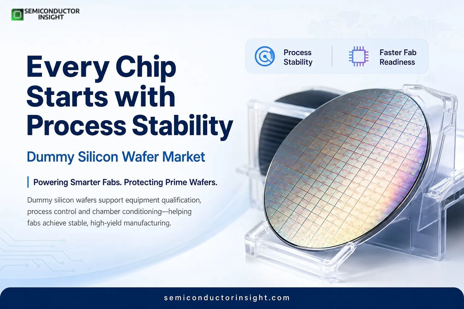
A dummy silicon wafer may never leave a semiconductor fabrication line as a finished electronic device, but it plays an important role in keeping manufacturing processes stable. These wafers are used for equipment qualification, process conditioning, chamber cleaning support, deposition experiments, alignment checks and other activities where manufacturers need a silicon surface without consuming a valuable production wafer.
The distinction is becoming increasingly important as semiconductor manufacturing moves toward tighter process windows. Modern fabs routinely work with wafers as large as 300mm in diameter, while advanced production is becoming increasingly automated and data-driven.
For More Detailed Insights, You Can Surf Our Latest Report Here: https://semiconductorinsight.com/report/dummy-silicon-wafer-market/
Why 300mm Is Changing the Conversation?
- The movement toward larger wafer formats is one of the clearest developments influencing the dummy wafer ecosystem.
- A 300mm wafer provides a substantially larger processing surface than a 200mm wafer, making it the dominant format for many high-volume semiconductor processes.
- The scale of current manufacturing investment illustrates the importance of this format. SEMI’s Q2 2026 outlook tracks 413 fabs and production lines worldwide, including R&D and pilot lines, and forecasts global 300mm front-end equipment spending of US$142 billion in 2026.
- Installed 300mm capacity is also projected to increase by 7% during 2026.
- For dummy wafer suppliers, expanding 300mm capacity means more opportunities to supply wafers used before, between and around production runs.
AI Chips Are Increasing the Value of Process Stability
The rapid expansion of AI computing is affecting the dummy silicon wafer market indirectly but significantly. Advanced logic and high-bandwidth memory manufacturing require exceptionally controlled deposition, etching, lithography and cleaning environments.
Worldwide silicon wafer shipments reached 3,275 million square inches in Q1 2026, representing a 13.1% year-over-year increase. SEMI attributed the improvement partly to continued demand associated with AI data centers, advanced logic and memory.
As more advanced wafers move through fabs, manufacturers have greater incentive to reserve production-grade substrates for actual device fabrication and use lower-cost dummy substrates for qualification and process-support activities.
Inside the Fab Where Dummy Wafers Earn Their Keep
Dummy wafers can be used at several stages of semiconductor manufacturing. Process engineers may run them through deposition chambers to stabilize equipment conditions, evaluate film formation, check wafer handling and validate process recipes before introducing product wafers.
They can also be used during equipment installation and qualification. This is particularly useful when a new tool has to be integrated into an automated production environment. Running dummy substrates allows engineers to verify mechanical handling and process behavior without putting customer product at unnecessary risk.
The value is therefore less about the wafer itself and more about the production time, yield protection and process information it helps generate.
The Economics behind Reusable Process Wafers
- Dummy wafers also have a practical economic role. Semiconductor manufacturers operate extremely expensive equipment, and an unplanned process excursion can affect multiple production lots.
- A reusable or reclaimable dummy wafer can therefore function as a relatively inexpensive process-development asset compared with consuming a high-value prime wafer for every equipment check or experimental run.
- The industry is also becoming more attentive to wafer utilization. SUMCO reported that AI and data-science initiatives at one of its main 300mm wafer plants improved total wafer production by more than 10%, demonstrating how even incremental efficiency gains can have substantial manufacturing value.
Advanced Nodes Are Raising the Standard for Surface Quality
As semiconductor geometries become smaller, the quality requirements placed on silicon substrates become increasingly demanding. Flatness, surface roughness, cleanliness, crystal quality and particle control all influence how wafers behave during processing.
This is relevant to dummy wafers because a process-support wafer still needs to behave predictably inside manufacturing equipment. A poorly controlled substrate can introduce contamination, particles or inconsistent process conditions and undermine the very qualification exercise it is intended to support.
This is why dummy wafers are increasingly viewed as process-enabling materials rather than disposable pieces of silicon.
2nm Production Adds a New Process-Control Dimension
The transition toward 2nm manufacturing provides a current example of how process qualification requirements are evolving. TSMC began volume production of its N2 technology in Q4 2025, while N2P production is scheduled for the second half of 2026. Its N2 platform uses nanosheet transistor technology and is designed to improve performance and power efficiency.
TSMC’s 2025 annual report also recorded 15.0 million 12-inch equivalent wafer shipments and noted that advanced technologies at 7nm and beyond represented 74% of total wafer revenue.
Such advanced manufacturing environments require repeated equipment qualification, process monitoring and recipe optimization, creating a wider role for dummy substrates.
Regional Fab Expansion Is Broadening the Customer Base
- The dummy silicon wafer opportunity is no longer limited to established Asian semiconductor clusters. New fabs and production lines are being developed across the United States, Europe, Japan and other locations as manufacturers diversify supply chains.
- TSMC is expanding production capacity in Taiwan while advancing facilities in Arizona, Japan and Germany. Its Arizona expansion is intended to support advanced logic production for smartphone, AI and high-performance computing applications.
- Every new production line requires equipment installation, qualification and process ramping before reaching stable high-volume manufacturing. This creates recurring demand for wafers used during those preparatory stages.
The Shift toward Smarter Wafer Utilization
The next phase of the dummy silicon wafer market is increasingly connected with automated fabs, higher wafer diameters and tighter process control. Manufacturers are seeking ways to protect expensive production substrates while collecting reliable process data during equipment qualification and maintenance.
With 300mm capacity expanding and AI-related semiconductor manufacturing continuing to attract investment, dummy wafers are becoming an understated but necessary component of the modern fab ecosystem. Their importance comes not from producing chips themselves, but from helping manufacturers reach stable, repeatable and high-yield production without unnecessarily consuming prime wafers.

Comments (0)