Water-Efficient Semiconductor Fab Market Insights
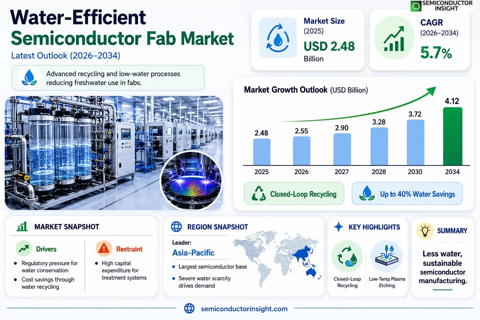
Global water-efficient semiconductor fab market size was valued at USD 2.48 billion in 2025. The market is projected to grow from USD 2.55 billion in 2026 to USD 4.12 billion by 2034, exhibiting a CAGR of 5.7% during the forecast period.
Water-efficient semiconductor fabs employ advanced process integration, closed‑loop water recycling, and low‑temperature plasma etching to minimize freshwater usage while maintaining high‑volume manufacturing yields. These technologies encompass reclaimed‑water treatment systems, dry‑strip cleaning, and innovative cooling architectures that together reduce total water consumption per wafer by up to 40% compared with conventional fabs.The market is gaining momentum because rising environmental regulations, escalating water scarcity in key manufacturing hubs such as Taiwan, South Korea, and the United States, and increasing corporate sustainability commitments are driving fab owners to adopt water‑saving solutions. Moreover, equipment vendors like Applied Materials, Lam Research, and Tokyo Electron are expanding their portfolios with water‑efficient modules, further accelerating adoption across the industry.
MARKET DRIVERS
Regulatory Pressure for Water Conservation
The increasing stringency of environmental regulations worldwide compels semiconductor manufacturers to adopt water‑efficient processes. Facilities that meet or exceed local water‑usage limits can avoid costly fines and gain preferential treatment in permitting, driving rapid adoption of closed‑loop water systems.
Cost Savings through Recycling
Recycling and reclamation technologies enable fabs to reduce fresh‑water purchases by up to 30 %, translating into multi‑million‑dollar annual savings for large plants. The financial upside is reinforced by lower wastewater treatment fees.
➤ “Investments in water‑efficient equipment have shortened payback periods to under two years in mature markets.”
In addition, consumer and investor demand for greener electronics pushes chipmakers to highlight water‑efficiency metrics, strengthening brand reputation and market share.
MARKET CHALLENGES
Technical Integration Barriers
Existing fab lines were designed around open‑loop cooling and rinse cycles. Retrofitting these facilities with water‑recycling modules often requires major downtime and specialized engineering expertise.
Other Challenges
Infrastructure Compatibility
Legacy piping, pumps, and sensor networks may not support the higher purity standards needed for reclaimed water, necessitating costly upgrades.
MARKET RESTRAINTS
High Capital Expenditure
Deploying advanced water‑treatment units such as reverse‑osmosis membranes or ion‑exchange columns involves substantial upfront investment. Smaller foundries often lack the financial bandwidth to fund these projects without external subsidies.Furthermore, the uncertainty around return on investment,particularly in regions with low water tariffs,deters some players from committing significant budgets to water‑efficiency upgrades.
MARKET OPPORTUNITIES
Advanced Membrane Technologies
Emerging nanofiltration membranes promise higher rejection rates for contaminants while consuming less energy than traditional reverse‑osmosis systems. Early adopters can capture additional water savings of 5‑10 % beyond current benchmarks.The growing prevalence of AI‑driven process control offers another avenue: predictive algorithms can dynamically adjust water‑reuse cycles, minimizing waste and increasing throughput without sacrificing yield.Geographically, regions experiencing water scarcity,such as parts of East Asia and the United States Southwest,present a ripe market for turnkey water‑efficient fab solutions, encouraging cross‑border collaborations and technology licensing.
Water-Efficient Semiconductor Fab Market Trends
Advanced Water Recycling Integration
Water-Efficient Semiconductor Fab Market is being reshaped by the rapid deployment of closed‑loop water recycling systems. Modern fabs now embed reclaimed‑water treatment modules directly into the process line, allowing fresh‑water substitution rates that approach 60 % for cooling and wafer‑processing steps. Coupled with low‑temperature plasma etching, these solutions cut total water consumption per wafer by up to 40 % without compromising cycle time or yield. Early adopters report measurable reductions in utility costs and improved compliance with local discharge limits, positioning water‑efficient designs as a baseline rather than a niche capability.
Other Trends
Regulatory Pressure and Corporate Sustainability
Regulators in Taiwan, South Korea, and key U.S. manufacturing corridors have introduced tighter water‑use permits, prompting fab owners to prioritize conservation measures. At the same time, global sustainability frameworks encourage semiconductor manufacturers to set science‑based targets for water stewardship. The convergence of policy and corporate ambition creates a compelling business case for retrofitting existing plants and designing new facilities around water‑saving architectures. Operators are increasingly tracking water‑intensity metrics alongside traditional productivity indicators, and internal dashboards now flag deviations that could trigger compliance actions.
Vendor-Driven Technology Expansion
Equipment suppliers such as Applied Materials, Lam Research, and Tokyo Electron are expanding their portfolios with dedicated water‑efficient modules. These offerings include dry‑strip cleaning stations that eliminate rinse cycles, innovative cooling towers that recycle condensate, and smart‑control software that dynamically balances freshwater draw against recycled supply. By integrating these technologies into standard process kits, vendors reduce the engineering overhead for fab managers and accelerate the rollout of water‑saving practices across the supply chain. The cumulative effect is a broader diffusion of best‑in‑class water management, reinforcing the overall momentum of the Water‑Efficient Semiconductor Fab Market.
COMPETITIVE LANDSCAPEKey Industry Players
Water‑Efficient Semiconductor Fab Market Competitive Overview
The water‑efficient semiconductor fab market is presently anchored by a handful of global equipment suppliers that have integrated closed‑loop water recycling and low‑temperature plasma etching into their process portfolios. Applied Materials leads the segment with its Water‑Smart™ module suite, which combines reclaimed‑water treatment and dry‑strip cleaning to achieve up to 35 % freshwater reduction per wafer. Lam Research follows closely, offering the Aqua‑Clean™ line that embeds inline water‑purification within deposition tools. Tokyo Electron’s EcoFab platform adds a modular cooling architecture that further curtails water draw. Market structure reflects a tiered model: Tier‑1 vendors supply core equipment, while fab operators such as Taiwan Semiconductor Manufacturing Company (TSMC) and Samsung Electronics adopt these solutions at scale, driving demand for higher‑efficiency retrofits across existing fabs.Beyond the dominant Tier‑1 vendors, a cohort of niche but strategically important players is expanding the competitive landscape. KLA Corporation provides advanced metrology tools that operate with reduced coolant flow, enhancing overall fab water efficiency. Veolia Water Technologies and SUEZ Water Technologies deliver turnkey reclaimed‑water treatment plants that are increasingly packaged with fab construction contracts. Smaller innovators such as Aquatech and Fluor Engineering contribute specialized membrane filtration and heat‑exchange designs, respectively, enabling fabs to approach near‑zero fresh‑water consumption. These companies, while not primary equipment manufacturers, create essential ancillary value that amplifies the impact of water‑saving initiatives and diversifies the supplier ecosystem.
List of Key Semiconductor Fab Companies Profiled
- Applied Materials
- Lam Research
- Tokyo Electron
- KLA Corporation
- TSMC
- Samsung Electronics
- Intel Corporation
- Veolia Water Technologies
- SUEZ Water Technologies
- Aquatech
- Fluor Engineering
- ASML Holding
- GlobalFoundries
Segment Analysis:
| Segment Category | Sub-Segments | Key Insights |
| By Type |
|
Closed‑Loop Recycling Systems
|
| By Application |
|
Advanced Logic Devices
|
| By End User |
|
Fab Operators
|
| By Technology |
|
Low‑Temperature Plasma Etching
|
| By Sustainability Initiative |
|
Zero‑Waste Water Strategies
|
Regional Analysis: North America
United States
The implementation of sophisticated water purification and recycling systems is a key trend. These technologies significantly reduce freshwater intake and minimize wastewater discharge.
Increasingly strict environmental regulations are driving the adoption of water-efficient practices. Compliance with these regulations is becoming a critical factor for semiconductor manufacturers.
The adoption of closed-loop water systems, where water is continuously recycled within the manufacturing process, is gaining momentum. This minimizes water consumption and reduces environmental impact.
Government programs and financial incentives are supporting the development and adoption of water-efficient semiconductor fab technologies.
Europe
The European market for water-efficient semiconductor fab solutions is characterized by a strong emphasis on sustainability and environmental responsibility. Stringent water regulations across various European Union member states are driving the adoption of innovative water management technologies within the semiconductor industry. The region’s strong focus on circular economy principles further supports the growth of water recycling and reuse initiatives. Several semiconductor manufacturers in Europe are actively collaborating with technology providers to implement advanced water treatment systems and optimize water usage in their fabrication facilities. The demand for these solutions is expected to rise steadily as water scarcity becomes a more pressing concern in several parts of Europe. Furthermore, research and development efforts are focused on developing next-generation water-efficient technologies that can further minimize the environmental impact of semiconductor manufacturing. The interplay between regulatory pressure and corporate sustainability goals creates a favorable environment for the growth of Water-Efficient Semiconductor Fab Market in Europe.
Asia-Pacific
Asia-Pacific represents the largest and fastest-growing market for water-efficient semiconductor fab solutions. The region’s burgeoning semiconductor industry, particularly in countries like Taiwan, South Korea, and China, is driving significant demand for these technologies. Rapid industrialization and increasing water stress in several parts of the region are further fueling market growth. Semiconductor manufacturers in Asia-Pacific are investing heavily in advanced water treatment systems, water recycling technologies, and optimized water usage practices. Government initiatives promoting sustainable manufacturing and attracting foreign investment in the semiconductor sector are also contributing to market expansion. The focus on reducing water footprint is often intertwined with efforts to improve overall operational efficiency. The sheer scale of semiconductor production in Asia-Pacific ensures a robust and sustained demand for water-efficient semiconductor fab solutions.
South America
Water-Efficient Semiconductor Fab Market in South America is in its nascent stages but holds significant growth potential. While the semiconductor industry in the region is relatively smaller compared to other regions, increasing investment in electronics manufacturing and a growing awareness of environmental sustainability are creating opportunities for water-efficient solutions. Water scarcity is a concern in several South American countries, making water conservation a priority. Initial adoption of advanced water treatment technologies is expected to be driven by larger semiconductor manufacturers and those aligning with global sustainability standards. Government policies promoting green technologies and attracting foreign semiconductor investments will play a crucial role in accelerating market growth. The focus will likely be on cost-effective water recycling and reuse solutions initially.
Middle East & Africa
The Middle East & Africa region presents a unique set of challenges and opportunities for Water-Efficient Semiconductor Fab Market. Water scarcity is a critical issue across this region, driving a strong need for advanced water management technologies. While the semiconductor industry is not as established as in other regions, there is growing investment in electronics manufacturing, particularly in countries like Saudi Arabia and South Africa. The focus on sustainable development and water conservation initiatives are creating a favorable environment for the adoption of water-efficient solutions. Investments in desalination technologies and water recycling systems are likely to be key components of Water-Efficient Semiconductor Fab Market in this region. The potential for growth is significant, driven by both government initiatives and the increasing demand from the expanding semiconductor sector.
Report Scope
This market research report provides a comprehensive analysis of the Water-Efficient Semiconductor Fab Market , covering the forecast period 2026–2034. It offers detailed insights into market dynamics, technological advancements, competitive landscape, and key trends shaping the industry.
Key focus areas of the report include:
- Market Overview: The report begins with an overview outlining its current market scenario, key growth indicators, and industry transformation drivers. It discusses macroeconomic factors, demand–supply balance, regulatory landscape, and the strategic role of semiconductors in powering advancements across industries such as automotive, telecommunications, consumer electronics, and industrial automation.
- Market Size & Forecast: Historical data and future projections for revenue, unit shipments, and market value across major regions and segments.
- Segmentation Analysis: Detailed breakdown by product type, technology, application, and end-user industry to identify high-growth segments and investment opportunities.
- Regional Insights: Insights into market performance across North America, Europe, Asia-Pacific, Latin America, and the Middle East & Africa, including country-level analysis where relevant.
- Competitive Landscape: Profiles of leading market participants, including their product offerings, R&D focus, manufacturing capacity, pricing strategies, and recent developments such as mergers, acquisitions, and partnerships.
- Technology Trends & Innovation: Assessment of emerging technologies, integration of AI/IoT, semiconductor design trends, fabrication techniques, and evolving industry standards.
- Market Drivers & Restraints: Evaluation of factors driving market growth along with challenges, supply chain constraints, regulatory issues, and market-entry barriers.
- Stakeholder Insights: Insights for component suppliers, OEMs, system integrators, investors, and policymakers regarding the evolving ecosystem and strategic opportunities.
Primary and secondary research methods are employed, including interviews with industry experts, data from verified sources, and real-time market intelligence to ensure the accuracy and reliability of the insights presented.
FREQUENTLY ASKED QUESTIONS:
What is the current market size of Water-Efficient Semiconductor Fab Market?
-> Water-Efficient Semiconductor Fab Market was valued at USD 2.48 billion in 2025 and is expected to reach USD 4.12 billion by 2034, reflecting a CAGR of 5.7% over the forecast period.
Which key companies operate in Water-Efficient Semiconductor Fab Market?
-> Key players include Applied Materials, Lam Research, and Tokyo Electron, among others.
What are the key growth drivers?
-> Key growth drivers include stringent environmental regulations, escalating water scarcity in major fab hubs, and increasing corporate sustainability commitments.
Which region dominates the market?
-> Asia-Pacific is the fastest‑growing region, while North America remains a dominant market due to a high concentration of advanced semiconductor manufacturing facilities.
What are the emerging trends?
-> Emerging trends include closed‑loop water recycling, low‑temperature plasma etching, and dry‑strip cleaning technologies that can reduce water consumption per wafer by up to 40%.

Get Sample Report PDF for Exclusive Insights
Report Sample Includes
- Table of Contents
- List of Tables & Figures
- Charts, Research Methodology, and more...
 Download Sample Report PDF