MARKET INSIGHTS
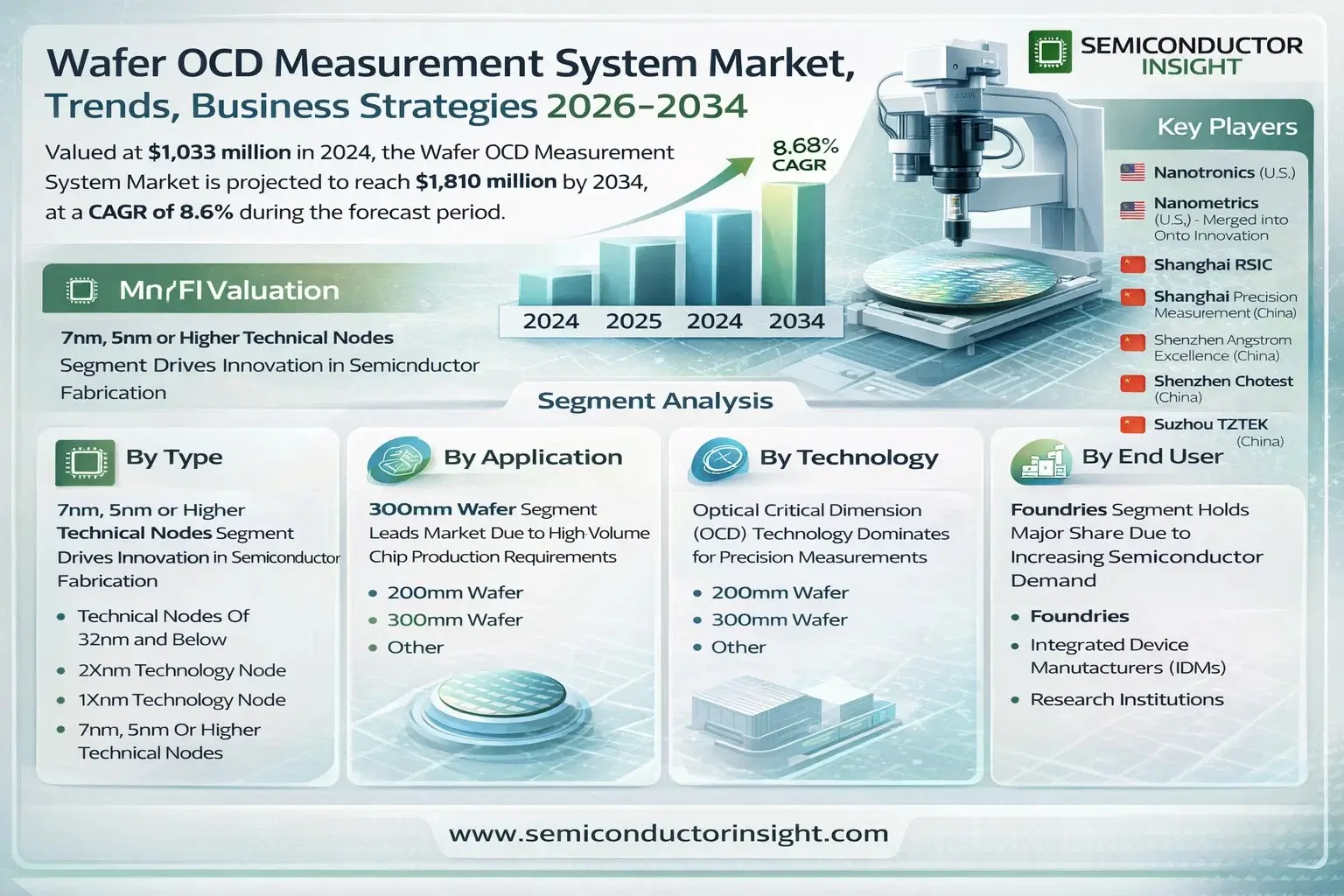
Global Wafer OCD Measurement System Market was valued at 1033 million in 2026 and is projected to reach USD 1810 million by 2034, at a CAGR of 8.6% during the forecast period.
Wafer OCD (Optical Critical Dimension) measurement systems are precision instruments used in semiconductor manufacturing to detect and analyze defects at nanometer-scale dimensions throughout the production process. These systems utilize advanced optical technologies to measure critical parameters such as film thickness, line width, and pattern profiles, ensuring higher yield and quality control in chip fabrication. The increasing complexity of semiconductor nodes, particularly in the transition to sub-7nm technologies, has heightened demand for these systems.
Growth in this market is primarily driven by the expansion of the semiconductor industry, particularly in Asia-Pacific regions like China, Taiwan, and South Korea, which collectively account for over 70% of global semiconductor equipment demand. Furthermore, technological advancements in AI, 5G, and electric vehicles are accelerating investments in semiconductor manufacturing, creating sustained demand for wafer metrology solutions. Key players such as KLA, NOVA, and Onto Innovation continue to innovate, with recent developments focusing on enhancing measurement precision for next-generation chips.
MARKET DYNAMICS
MARKET DRIVERS
Semiconductor Industry Expansion and Advanced Node Development Driving Demand
Global semiconductor industry’s relentless pursuit of smaller process nodes is creating unprecedented demand for Wafer OCD Measurement Systems. As manufacturers push technological boundaries with 5nm and below fabrication processes, the need for precise metrology solutions has become critical. These systems provide essential dimensional and material property measurements during chip manufacturing, helping achieve higher yields in advanced semiconductor production. The market is being propelled by massive investments in semiconductor fabrication plants, with over 80 new facilities projected to come online worldwide by 2030, requiring sophisticated metrology solutions.
AI and HPC Applications Creating New Demand Drivers
Artificial intelligence and high-performance computing applications are reshaping semiconductor requirements and consequently boosting the OCD measurement market. The complex architectures of AI chips require extremely precise manufacturing controls, with OCD systems playing a crucial role in ensuring performance uniformity across wafers. Demand from data center operators and cloud service providers has grown exponentially, with AI chip production volumes projected to increase by over 40% annually through 2030. Major foundries are expanding capacity to meet this demand, directly benefiting OCD system manufacturers.
MARKET RESTRAINTS
High Initial Costs and ROI Challenges for Small Manufacturers
While Wafer OCD Measurement Systems are essential for leading-edge semiconductor production, their high costs present significant barriers to adoption. Advanced systems can cost millions of dollars, making them prohibitive for smaller manufacturers or those working with mature nodes. The total cost of ownership includes not just the equipment but also specialized maintenance, calibration, and operator training. For companies producing less sophisticated chips, the return on investment timeline often appears too long, despite the potential yield benefits these systems could provide.
Integration Complexities with Existing Fab Infrastructure
Integrating new OCD measurement systems with existing fabrication lines presents considerable challenges. Many semiconductor facilities operate on tight production schedules where equipment downtime can cost millions per day. Retrofitting older fabs to accommodate new metrology tools requires careful planning and significant capital expenditure. Additionally, compatibility issues with various process control software platforms can create bottlenecks, slowing down the adoption of newer measurement technologies even when they offer technical advantages.
MARKET CHALLENGES
Shortage of Skilled Metrology Professionals Creating Bottlenecks
The semiconductor industry faces an acute shortage of professionals trained in advanced metrology techniques. Operating modern OCD measurement systems requires specialized knowledge of optics, materials science, and semiconductor physics that isn’t widely available. Educational institutions have struggled to keep pace with industry demands, resulting in intense competition for qualified personnel. This talent gap has forced some manufacturers to delay equipment deployments despite having made capital investments.
Measurement Accuracy Challenges at Advanced Nodes
As semiconductor features shrink below 5nm, OCD measurement systems face fundamental physics challenges in maintaining accuracy. The industry is approaching dimensional scales where quantum effects begin influencing measurement reliability. Manufacturers must constantly validate and recalibrate systems to account for these phenomena. This not only increases operational costs but also creates uncertainty in production control, potentially affecting yield predictions and fabrication timelines.
MARKET OPPORTUNITIES
Expansion in Emerging Semiconductor Markets Creates New Growth Avenues
Government initiatives worldwide to develop domestic semiconductor capabilities are creating significant opportunities for Wafer OCD Measurement System providers. Major economies have announced over D 200 billion in combined semiconductor industry incentives, with much of this investment targeting advanced manufacturing capabilities. These new facilities will require comprehensive metrology solutions, presenting OEMs with fresh markets beyond traditional semiconductor hubs. Growth potential is particularly strong in Southeast Asia and North America where new fab construction is most active.
Development of Integrated Metrology Solutions for Smart Factories
The industry shift toward smart manufacturing and Industry 4.0 practices is driving demand for OCD systems with enhanced data integration capabilities. Manufacturers seek solutions that can interface seamlessly with factory automation systems and provide real-time process adjustments. This trend has prompted equipment makers to develop AI-enhanced measurement tools capable of predictive analytics and autonomous decision-making. Such advanced systems command premium pricing and create opportunities for recurring revenue through software and service offerings.
WAFER OCD MEASUREMENT SYSTEM MARKET TRENDS
Increasing Demand for Advanced Semiconductor Nodes to Drive Market Growth
Global Wafer OCD Measurement System Market is witnessing significant growth due to the rising demand for advanced semiconductor nodes, particularly below 7nm. With semiconductor manufacturers striving for higher performance and energy efficiency, the need for precise metrology solutions like OCD (Optical Critical Dimension) has become critical. The market is projected to grow at a CAGR of 8.6%, from D 1,033 million in 2026 to D 1,810 million by 2034, as semiconductor fabs expand their production capabilities to meet the needs of AI, 5G, and high-performance computing applications. Key regions such as China, Taiwan, and South Korea now hold a combined 70% market share, driven by aggressive semiconductor manufacturing expansions.
Other Trends
Integration of AI and Machine Learning for Enhanced Precision
AI and machine learning are transforming Wafer OCD measurement systems by improving defect detection accuracy and reducing process variability. Leading manufacturers are leveraging deep learning algorithms to analyze complex wafer patterns in real-time, enabling faster yield optimization. This technological shift is particularly beneficial for cutting-edge nodes like 5nm and below, where even nanometer-scale deviations can impact chip performance. The adoption of smart metrology solutions is expected to accelerate further as semiconductor firms seek to minimize production delays and scrap rates.
Expansion of 300mm Wafer Production and EV Market Influence
The transition towards 300mm wafer production is reshaping the OCD measurement landscape, as larger wafers demand more sophisticated inspection systems. The 300mm wafer segment dominates the market with over 60% adoption, catering to high-volume chip manufacturing for data centers and automotive applications. The electric vehicle (EV) boom is further propelling demand, with semiconductor content in EVs estimated to be twice that of conventional vehicles. As automakers increase investments in self-driving and connectivity technologies, semiconductor suppliers are expanding their wafer fabrication capacities, driving the need for advanced metrology solutions.
COMPETITIVE LANDSCAPE
Key Industry Players
Strategic Investments in Advanced Metrology Solutions Reshape Competitive Dynamics
Wafer OCD Measurement System Market exhibits a moderately consolidated competitive landscape, with KLA Corporation dominating nearly 35% of the global market share in 2026. This leadership stems from their proprietary optical critical dimension (OCD) technology and extensive semiconductor industry partnerships across key manufacturing hubs in Taiwan, South Korea, and the United States.
Onto Innovation and NOVA follow closely, collectively accounting for approximately 28% of market revenue, as confirmed by recent financial disclosures. These companies have gained traction through their comprehensive solutions for advanced node measurement, particularly for sub-7nm process technologies where precision requirements are most stringent.
While established players maintain dominance, Chinese manufacturers like Shanghai RSIC and Shenzhen Angstrom Excellence are aggressively expanding their market presence through government-backed semiconductor initiatives. Their growth strategies focus on cost-competitive alternatives for mature nodes while gradually enhancing capabilities for leading-edge applications.
The competitive intensity is further heightened by recent technological pivots – Nanometrics merged with Rudolph Technologies in 2020 to form Onto Innovation, creating a stronger product portfolio. Meanwhile, KLA continues to leverage its acquisition of Orbotech to integrate wafer inspection and metrology solutions, offering customers end-to-end process control capabilities.
List of Key Wafer OCD Measurement System Manufacturers
- KLA Corporation (U.S.)
- Onto Innovation (U.S.)
- NOVA (Israel)
- Nanotronics (U.S.)
- Nanometrics (U.S.) – Merged into Onto Innovation
- Shanghai RSIC (China)
- Shanghai Precision Measurement (China)
- Shenzhen Angstrom Excellence (China)
- Shenzhen Chotest (China)
- Suzhou TZTEK Technology (China)
Segment Analysis:
By Type
7nm, 5nm or Higher Technical Nodes Segment Drives Innovation in Semiconductor Fabrication
The market is segmented based on type into:
- Technical Nodes Of 32nm and Below
- 2Xnm Technology Node
- 1Xnm Technology Node
- 7nm, 5nm Or Higher Technical Nodes
By Application
300mm Wafer Segment Leads Market Due to High-Volume Chip Production Requirements
The market is segmented based on application into:
- 200mm Wafer
- 300mm Wafer
- Other
By Technology
Optical Critical Dimension (OCD) Technology Dominates for Precision Measurements
The market is segmented based on technology into:
- Optical Critical Dimension (OCD)
- Scatterometry
- Spectroscopic Ellipsometry
- Others
By End User
Foundries Segment Holds Major Share Due to Increasing Semiconductor Demand
The market is segmented based on end user into:
- Foundries
- Integrated Device Manufacturers (IDMs)
- Research Institutions
Regional Analysis: Wafer OCD Measurement System Market
North America
The North American market for Wafer OCD Measurement Systems is driven by strong semiconductor R&D investments and increasing demand for advanced chip manufacturing technologies. The U.S., home to leading semiconductor companies like Intel and AMD, accounted for over 70% of the region’s market share in 2026. Government initiatives such as the CHIPS and Science Act, which allocated D 52 billion for domestic semiconductor production, are accelerating innovation and adoption of precision metrology tools. However, high equipment costs and supply chain dependencies on Asia remain key challenges. The focus is shifting toward 7nm and below node technologies, with strong demand from AI and automotive semiconductor applications.
Europe
Europe maintains a steady position in the Wafer OCD Measurement System Market, mainly due to specialized semiconductor fabs in Germany and the Netherlands. The region is witnessing growing adoption driven by automotive electrification and IoT applications, though market penetration remains lower than in Asia. Collaborative initiatives like the EU Chips Act, which aims to mobilize €43 billion in public and private investments, are expected to strengthen local supply chains. European manufacturers emphasize sustainability and energy efficiency, influencing the development of next-generation metrology solutions. However, limited scale in leading-edge node production restricts high-volume demand.
Asia-Pacific
Asia-Pacific dominates the global market, with China, Taiwan, and South Korea collectively accounting for over 70% of global semiconductor equipment spending. China’s aggressive push for semiconductor self-sufficiency, backed by government subsidies and expanding foundries, is fueling demand for OCD measurement systems. Taiwan remains critical due to TSMC’s leadership in 5nm and 3nm process technologies, requiring ultra-high-precision metrology. Meanwhile, South Korea’s Samsung and SK Hynix drive adoption through advanced memory production. Despite geopolitical tensions affecting supply chains, the region continues to innovate, particularly in 3D NAND and logic device manufacturing.
South America
South America’s market for Wafer OCD Measurement Systems is in early stages, with limited semiconductor manufacturing infrastructure. Brazil shows modest growth in microelectronics, primarily for industrial and automotive applications. The lack of a developed foundry ecosystem and reliance on imported equipment constrain market expansion. However, government incentives for local semiconductor R&D, though minimal compared to global standards, could create niche opportunities in sensor and analog chip production. Economic instability and inadequate funding for high-tech industries remain barriers to sustainable growth in the region.
Middle East & Africa
The Middle East & Africa region represents an emerging opportunity, primarily driven by UAE and Saudi Arabia’s technology diversification strategies. Investments in smart city projects and local semiconductor hubs, such as Saudi Arabia’s D 20 billion semiconductor fund, could stimulate demand for metrology tools in the long term. However, the absence of established fabs and reliance on foreign suppliers limit immediate market potential. Africa, while lacking semiconductor manufacturing capabilities, is witnessing gradual tech-sector growth, with wafer testing services gaining traction in South Africa and Egypt.
Report Scope
This market research report provides a comprehensive analysis of the Global Wafer OCD Measurement System Market, covering the forecast period 2026–2034. It offers detailed insights into market dynamics, technological advancements, competitive landscape, and key trends shaping the semiconductor metrology industry.
Key focus areas of the report include:
- Market Size & Forecast: Historical data and future projections for revenue, unit shipments, and market value across major regions and segments. The market was valued at USD 1,033 million in 2026 and is projected to reach USD 1,810 million by 2034 at a CAGR of 8.6%.
- Segmentation Analysis: Detailed breakdown by technology node (32nm and below, 2Xnm, 1Xnm, 7nm/5nm and higher) and wafer size (200mm, 300mm, others) to identify high-growth segments.
- Regional Outlook: Insights into market performance across North America, Europe, Asia-Pacific, Latin America, and Middle East & Africa. Asia-Pacific dominates with over 70% market share, led by semiconductor hubs in China, Taiwan, and South Korea.
- Competitive Landscape: Profiles of leading market participants including KLA, NOVA, Onto Innovation, Nanometrics and emerging Chinese players, analyzing their product portfolios, R&D investments, and strategic moves.
- Technology Trends & Innovation: Assessment of advanced metrology solutions integrating AI/ML for defect detection, multi-channel measurement systems, and solutions for advanced nodes below 5nm.
- Market Drivers & Restraints: Evaluation of growth drivers like HPC, AI chips, 5G, and electric vehicles, along with challenges such as trade restrictions and high R&D costs.
- Stakeholder Analysis: Strategic insights for foundries, IDMs, equipment suppliers, and investors regarding technology adoption and market opportunities.
The research methodology combines primary interviews with semiconductor equipment experts, analysis of financial reports from key players, and validation through secondary sources to ensure data accuracy.
FREQUENTLY ASKED QUESTIONS:
What is the current market size of Global Wafer OCD Measurement System Market?
-> Wafer OCD Measurement System Market was valued at 1033 million in 2026 and is projected to reach USD 1810 million by 2034, at a CAGR of 8.6% during the forecast period.
Which key companies operate in this market?
-> Key players include KLA, NOVA, Onto Innovation, Nanometrics, Nanotronics, along with emerging Chinese manufacturers like Shanghai RSIC and Shenzhen Angstrom Excellence.
What are the key growth drivers?
-> Primary drivers include advancement to sub-5nm nodes, increasing semiconductor complexity, and demand from AI/ML chip manufacturing.
Which region dominates the market?
-> Asia-Pacific holds over 70% market share, driven by semiconductor manufacturing in China, Taiwan, and South Korea.
What are the emerging trends?
-> Emerging trends include AI-powered defect detection, hybrid metrology solutions, and systems for 3D NAND and advanced packaging applications.

Get Sample Report PDF for Exclusive Insights
Report Sample Includes
- Table of Contents
- List of Tables & Figures
- Charts, Research Methodology, and more...