Wafer Level Bump Packaging and Testing Service Market, Size, Trends, Business Strategies 2026-2034

Global Wafer Level Bump Packaging and Testing Service Market was valued at USD 5,127 million in 2025 and is expected to reach USD 8,146 million by 2034, growing at a CAGR of 7.0% during the forecast period

PDF Icon Download Sample Report PDF
  • Quick Dispatch

    All Orders

  • Secure Payment

    100% Secure Payment

Price range: $1,500.00 through $4,250.00

Clear

Wafer Level Bump Packaging and Testing Service Market Insights

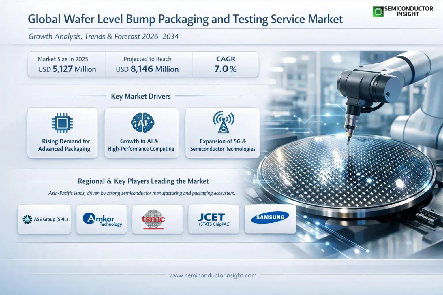
Global Wafer Level Bump Packaging and Testing Service market size was valued at USD 5,127 million in 2025. The market is projected to grow from USD 5,486 million in 2026 to USD 8,146 million by 2034, exhibiting a CAGR of 7.0% during the forecast period.

Wafer-level bumping packaging and testing service refers to an advanced technical service that packages and tests chips directly on wafers during the semiconductor manufacturing process. Metal bumps are directly formed on the wafers that have completed circuit manufacturing as the interconnection structure between the chip and the external circuit board. This service avoids the traditional steps of cutting individual chips before packaging, and can implement bump production, packaging, electrical performance testing, and visual inspection at the wafer level to reduce costs and improve production efficiency.

Wafer Level Bump Packaging and Testing Service, commonly referred to as wafer bumping, is a key process within advanced packaging ,a broad category of semiconductor packaging technologies that go beyond traditional wire bonding and plastic molding to enable higher performance, increased functionality, and better power efficiency. It integrates multiple chips, dies, or components into a single package using technologies such as Flip-Chip, Fan-Out Wafer-Level Packaging (FOWLP), 2.5D/3D Integration, System-in-Package (SiP), and Chiplet-based architectures. Global advanced packaging market is expected to surpass USD 79.1 billion by 2031, fueled by the adoption of heterogeneous integration and chiplet-based systems, underscoring the strategic importance of wafer bumping services. Major foundries such as TSMC, Intel, and Samsung, alongside leading OSATs including ASE, Amkor Technology, and JCET, are actively investing in high-density advanced packaging capabilities to meet the surging demand from AI accelerators, mobile processors, data center SoCs, and automotive electronics.

Wafer Level Bump Packaging and Testing Service Market Insights

MARKET DRIVERS

Rising Demand for Advanced Semiconductor Packaging in Consumer Electronics and High-Performance Computing

Wafer Level Bump Packaging and Testing Service Market is experiencing robust growth momentum, primarily driven by the accelerating adoption of advanced semiconductor packaging technologies across consumer electronics, data centers, and high-performance computing platforms. As device miniaturization continues to push the boundaries of traditional packaging formats, wafer level bump packaging has emerged as a preferred interconnect solution, offering superior electrical performance, reduced form factor, and enhanced thermal management. The proliferation of smartphones, wearables, and IoT-enabled devices has created sustained upstream demand for wafer-level packaging services that can support high I/O density and fine-pitch bump structures.

Expansion of 5G Infrastructure and AI-Driven Chip Architectures Fueling Market Momentum

Global rollout of 5G networks and the rapid scaling of artificial intelligence workloads have significantly elevated the complexity and performance requirements of semiconductor chips, positioning wafer level bump packaging and testing services as critical enablers of next-generation connectivity. Advanced packaging formats such as flip-chip ball grid arrays (FC-BGA) and copper pillar bumping are increasingly integrated into RF front-end modules, application processors, and AI accelerators, all of which demand precision bump formation and rigorous electrical testing protocols. The shift toward heterogeneous integration and chiplet-based architectures further amplifies the need for reliable wafer-level interconnect and co-testing ecosystems.

As semiconductor nodes continue to shrink below 3nm and 2nm process geometries, wafer level bump packaging and testing service providers are investing heavily in ultra-fine pitch copper pillar and micro-bump technologies to meet the evolving performance benchmarks of leading fabless chip designers and integrated device manufacturers.

Collaborative developments between OSATs (Outsourced Semiconductor Assembly and Test companies) and foundries are reshaping the competitive landscape of Wafer Level Bump Packaging and Testing Service Market, with a clear trend toward integrated front-end and back-end process flows. This convergence is enabling faster time-to-market cycles and improved yield optimization, reinforcing the market’s long-term growth trajectory across automotive, aerospace, and medical electronics verticals.

MARKET CHALLENGES

Technical Complexity of Ultra-Fine Pitch Bump Formation and Yield Management

One of the most pressing challenges confronting participants in Wafer Level Bump Packaging and Testing Service Market is the increasing technical complexity associated with ultra-fine pitch bump deposition processes. As interconnect pitches shrink to sub-100 micron dimensions, maintaining dimensional uniformity, bump coplanarity, and solder joint integrity becomes exponentially more difficult. Process-induced defects such as bridging, voiding, and non-wetting failures directly impact yield rates, creating significant cost pressures for service providers operating on thin margins in a highly competitive environment. Advanced inspection and metrology solutions are required at every stage of the bump formation process, adding to capital expenditure burdens.f

Other Challenges

High Capital Investment Requirements

The establishment and continuous upgrading of wafer level bump packaging and testing infrastructure demands substantial capital outlay, encompassing electroplating equipment, advanced lithography tools, wafer probing systems, and automated optical inspection platforms. For mid-tier service providers in Wafer Level Bump Packaging and Testing Service Market, financing these investments while maintaining competitive pricing remains a structural challenge, particularly amid cyclical downturns in the broader semiconductor industry.

Supply Chain Disruptions and Materials Sourcing Constraints

Global semiconductor supply chain remains vulnerable to geopolitical tensions, trade restrictions, and raw material shortages, all of which directly affect the availability and pricing of specialty chemicals, photoresists, and electroplating materials essential to bump packaging processes. Service providers in Wafer Level Bump Packaging and Testing Service Market must develop resilient multi-source procurement strategies and maintain strategic material buffers to mitigate supply-side volatility without compromising delivery timelines or quality standards.

MARKET RESTRAINTS

Stringent Reliability Standards and Qualification Cycles Limiting Market Scalability

A significant restraint on Wafer Level Bump Packaging and Testing Service Market is the rigorous qualification and reliability certification process mandated by end-use industries such as automotive, aerospace, and medical electronics. Automotive-grade semiconductor components, governed by AEC-Q100 and IATF 16949 standards, require extensive thermal cycling, mechanical shock, and humidity endurance testing before commercial deployment, substantially extending product development timelines. These prolonged qualification cycles constrain the ability of wafer level packaging service providers to rapidly scale capacity in response to emerging demand signals, effectively creating a structural bottleneck in market responsiveness.

Concentration of Advanced Packaging Capabilities Among a Limited Number of Tier-1 Providers

Wafer Level Bump Packaging and Testing Service Market is characterized by a significant concentration of advanced technical capabilities and intellectual property among a small number of tier-1 OSATs and integrated device manufacturers. This concentration creates barriers to entry for emerging service providers and limits the negotiating leverage of fabless chip designers seeking diversified packaging supply chains. Regional disparities in advanced packaging infrastructure, particularly between East Asian markets and Western economies, further compound this restraint, as reshoring initiatives in North America and Europe face multi-year timelines before meaningful capacity becomes commercially available.

MARKET OPPORTUNITIES

Accelerating Adoption of Advanced Heterogeneous Integration Creating New Revenue Streams

Wafer Level Bump Packaging and Testing Service Market stands to benefit substantially from the industry-wide transition toward heterogeneous integration architectures, wherein multiple chiplets with diverse functional profiles are co-packaged within a single device footprint. This paradigm shift demands sophisticated wafer-level interconnect solutions, including hybrid bonding, through-silicon via (TSV) integration, and multi-tier bump structures, all of which fall within the core competency domain of advanced packaging service providers. As leading semiconductor companies across the United States, Taiwan, South Korea, and Europe accelerate chiplet roadmap execution, demand for specialized wafer level bump packaging and co-testing services is expected to expand across both volume production and engineering service engagements.

Government-Led Semiconductor Localization Initiatives Opening New Geographic Markets

Policy-driven semiconductor investment programs, including the U.S. CHIPS and Science Act, the European Chips Act, and analogous initiatives across India and Japan, are creating substantial greenfield opportunities for Wafer Level Bump Packaging and Testing Service Market. These programs provide direct funding, tax incentives, and research co-investment mechanisms that lower the capital risk threshold for establishing advanced packaging facilities in geographies that have historically lacked domestic wafer-level processing capabilities. Service providers positioned to align their capacity expansion strategies with these national semiconductor sovereignty agendas are likely to secure long-term anchor customer commitments, creating durable competitive advantages in newly emerging packaging ecosystems.

Growing Automotive Electrification and ADAS Adoption Driving Specialized Packaging Demand

The accelerating electrification of Global automotive fleet and the rapid advancement of advanced driver-assistance systems (ADAS) and autonomous driving technologies represent a high-value opportunity segment for Wafer Level Bump Packaging and Testing Service Market. Power management ICs, LiDAR sensing modules, radar processing chips, and in-vehicle networking semiconductors all require packaging solutions that combine high thermal conductivity, robust mechanical reliability, and fine-pitch electrical interconnects , precisely the performance envelope addressed by wafer level bump packaging technologies. As automotive semiconductor content per vehicle continues to rise, specialized bump packaging and functional testing services tailored to automotive-grade requirements are poised for sustained demand growth through the decade ahead.

MAIN TITLE HERE () Trends

Rising Demand from AI, HPC, and Advanced Packaging Adoption Drives Wafer Level Bump Packaging and Testing Service Market

Wafer Level Bump Packaging and Testing Service Market is experiencing significant momentum, largely driven by the accelerating adoption of advanced semiconductor packaging technologies across high-performance computing (HPC), artificial intelligence (AI), and data center applications. Wafer-level bumping, which involves forming metal interconnects directly on completed wafers before dicing, has emerged as a foundational process enabling higher I/O density, improved signal integrity, and reduced overall packaging costs. As chipmakers and OSATs scale investments in Flip-Chip, Fan-Out Wafer-Level Packaging (FOWLP), and 2.5D/3D integration architectures, demand for precision bumping and wafer-level testing services continues to grow steadily across global semiconductor supply chains.

The shift toward heterogeneous integration and chiplet-based system designs is reshaping packaging requirements. Technologies such as Copper Pillar Bumping (CPB), micro-bumps (uBump) for 2.5D/3D stacking, and Through-Silicon Via (TSV)-enabled interconnects are increasingly preferred over traditional solder bumps due to their superior electrical performance and finer pitch capabilities. Leading foundries including TSMC, Intel, and Samsung, alongside major OSAT players such as ASE, Amkor Technology, and JCET, are actively expanding their wafer bumping capacities to address next-generation computing and networking chip requirements. The transition to 12-inch wafer bumping from 8-inch formats is also gaining traction as manufacturers pursue economies of scale and higher throughput.

Other Trends

Expansion of Automotive and Industrial Applications

Wafer Level Bump Packaging and Testing Service Market is witnessing growing traction in automotive electronics and industrial applications. The proliferation of advanced driver-assistance systems (ADAS), electric vehicle (EV) power management chips, and ruggedized industrial sensors is pushing demand for reliable, high-precision wafer-level packaging and testing services. Automotive-grade semiconductor components require stringent electrical testing and thermal performance validation at the wafer level, making bumping and testing services an indispensable part of the supply chain for this segment.

Growth of Mobile and Consumer Device Segments

Mobile devices, PCs, laptops, and consumer IoT products continue to represent a substantial application base for wafer level bump packaging. The persistent miniaturization trend in mobile processors and display driver ICs (DDICs) is driving adoption of WLCSP and Bump for DDIC technologies. Chipmakers serving smartphone OEMs are increasingly relying on wafer-level packaging formats to achieve compact form factors while maintaining competitive power efficiency and processing performance.

Regional Capacity Expansion and Supply Chain Localization Shape Market Dynamics

Asia remains the dominant region for Wafer Level Bump Packaging and Testing Service activity, with China, South Korea, Japan, and Southeast Asia hosting a concentration of both OSAT facilities and integrated device manufacturers (IDMs). However, geopolitical considerations and supply chain resilience strategies are encouraging capacity investments in North America and Europe. Government-backed semiconductor initiatives are incentivizing domestic advanced packaging infrastructure, which is expected to gradually diversify Global footprint of wafer bumping and testing services over the coming years. Sustainability and design co-optimization between packaging and chip design teams are also emerging as key strategic priorities influencing service provider roadmaps.

COMPETITIVE LANDSCAPE

Key Industry Players

Wafer Level Bump Packaging and Testing Service Market , Competitive Dynamics, Strategic Positioning, and Leading OSAT & IDM Players

Global Wafer Level Bump Packaging and Testing Service market is characterized by a moderately consolidated competitive structure, dominated by a handful of large Outsourced Semiconductor Assembly and Test (OSAT) providers and Integrated Device Manufacturers (IDMs) with deep technological capabilities. ASE Group (inclusive of SPIL) commands a leading position in this space, leveraging its extensive flip-chip bumping lines, copper pillar bump (CPB) expertise, and high-volume 12-inch wafer bumping infrastructure. Amkor Technology and JCET (formerly STATS ChipPAC) follow closely, each offering a broad portfolio spanning FC Bumping, WLCSP, and advanced uBump technologies catering to AI accelerators, high-performance computing, and mobile applications. Major foundries such as TSMC, Samsung, and Intel have also deepened their involvement in wafer-level bumping as part of their advanced packaging strategies , integrating 2.5D/3D interposer-based packaging, Through-Silicon Via (TSV) stacking, and hybrid bonding into their process roadmaps. The market’s competitive intensity is further shaped by heavy capital investments in RDL Interposer, Fan-Out Wafer-Level Packaging (FOWLP), and co-packaged optics (CPO), particularly to support demand from data centers, 5G network infrastructure, and automotive electronics segments.

Beyond the tier-one players, a growing cohort of specialized and regionally significant companies is reshaping the competitive terrain of Wafer Level Bump Packaging and Testing Service Market. Powertech Technology Inc. (PTI), Tongfu Microelectronics (TFME), ChipMOS TECHNOLOGIES, and Chipbond Technology Corporation have established strong niches in DDIC bumping, WLCSP, and cost-competitive 8-inch wafer bumping services, serving consumer electronics, display driver IC, and IoT application segments. South Korean players such as Nepes, LB Semicon Inc., SFA Semicon, and Hana Micron are actively expanding their wafer bumping capabilities to capture demand from mobile and automotive customers, while Chinese OSATs including Hefei Chipmore Technology, Union Semiconductor (Hefei), Tongfu Microelectronics, Jiangsu CAS Microelectronics Integration, and Jiangsu Yidu Technology are scaling rapidly under government-supported semiconductor self-sufficiency initiatives. Emerging companies such as Ningbo ChipEx Semiconductor, Shenzhen TXD Technology, Raytek Semiconductor, Winstek Semiconductor, and International Micro Industries, Inc. (IMI) are carving out positions in niche bump types including CuNiAu and Gold Bump processes, further intensifying competitive pressure across mid-tier market segments.

List of Key Wafer Level Bump Packaging and Testing Service Companies Profiled

  • ASE Group (SPIL)
  • Amkor Technology
  • TSMC
  • JCET (STATS ChipPAC)
  • Intel Corporation
  • Samsung Electronics
  • SJSemi
  • ChipMOS TECHNOLOGIES
  • Chipbond Technology Corporation
  • Hefei Chipmore Technology
  • Union Semiconductor (Hefei) Co., Ltd.
  • HT-tech
  • Powertech Technology Inc. (PTI)
  • Tongfu Microelectronics (TFME)
  • Nepes
  • LB Semicon Inc.
  • SFA Semicon
  • International Micro Industries, Inc. (IMI)
  • Raytek Semiconductor
  • Winstek Semiconductor
  • Hana Micron
  • Ningbo ChipEx Semiconductor Co., Ltd.
  • UTAC Group
  • Shenzhen TXD Technology
  • Jiangsu CAS Microelectronics Integration
  • Jiangsu Yidu Technology

Segment Analysis:

Segment Category Sub-Segments Key Insights
By Type
  • FC Bumping (Flip-Chip Bumping)
  • WLCSP (Wafer Level Chip Scale Package)
  • uBump (2.5D/3D)
  • Bump for DDIC
  • Others
FC Bumping (Flip-Chip Bumping) holds the leading position in Wafer Level Bump Packaging and Testing Service Market by package technology, driven by its critical role in enabling high-density interconnects for advanced semiconductor devices.

  • Flip-chip bumping is extensively adopted across high-performance computing (HPC) platforms and AI accelerator chip packages, where superior electrical performance and thermal management are non-negotiable requirements.
  • The technology supports fine-pitch interconnection architectures that are indispensable for next-generation SoC designs, enabling seamless integration of logic, memory, and analog components within compact form factors.
  • Increasing demand for heterogeneous integration approaches and chiplet-based system architectures continues to reinforce FC Bumping as the preferred packaging method for leading foundries and OSATs investing in advanced packaging infrastructure.
By Application
  • Mobile Devices
  • PCs / Laptops / Tablets
  • Automotive
  • Servers, Data Centers & AI
  • Network Infrastructure
  • Industrial & Medical
  • Appliances / Consumer Goods / IoT
  • Others
Servers, Data Centers & AI represents the fastest-growing and increasingly dominant application segment within Wafer Level Bump Packaging and Testing Service Market, reflecting the explosive global appetite for artificial intelligence infrastructure and cloud computing capacity.

  • The proliferation of large language models, generative AI platforms, and high-bandwidth memory (HBM) requirements is compelling data center operators to source chips packaged through advanced wafer-level bumping processes that support extreme I/O density and signal integrity.
  • Advanced bump technologies such as uBump and copper pillar bumping are critically enabling 2.5D and 3D integration solutions used in AI accelerators, GPUs, and custom ASICs deployed across hyperscale data center environments.
  • Mobile Devices continues to be a significant volume-driven application segment, as smartphone OEMs increasingly demand miniaturized, high-performance processor packages that leverage WLCSP and flip-chip bumping for compact and power-efficient designs.
By End User
  • OSAT (Outsourced Semiconductor Assembly and Test)
  • IDM (Integrated Device Manufacturers)
  • Foundries
OSAT (Outsourced Semiconductor Assembly and Test) providers represent the leading end-user category in Wafer Level Bump Packaging and Testing Service Market, as fabless semiconductor companies and system designers increasingly outsource their advanced packaging requirements to specialized service providers.

  • Leading OSATs such as ASE (SPIL), Amkor Technology, and JCET (STATS ChipPAC) are making substantial capital investments in wafer-level bumping capacity to address surging demand from fabless chip designers who require turnkey packaging and testing solutions without in-house infrastructure.
  • IDMs and major foundries including TSMC, Intel, and Samsung are also significant participants, leveraging their vertically integrated manufacturing capabilities to offer wafer bumping services as part of comprehensive advanced packaging ecosystems, thereby intensifying competition and driving technological innovation across the value chain.
  • The rise of the chiplet ecosystem is encouraging both OSATs and foundries to collaborate on heterogeneous integration platforms, blurring traditional boundaries and creating new service models within the end-user landscape.
By Bump Type
  • Copper Pillar Bump (CPB)
  • Solder Bump
  • uBump (2.5D/3D)
  • CuNiAu Bumping
  • Gold Bump
  • Others
Copper Pillar Bump (CPB) is the dominant bump type in Wafer Level Bump Packaging and Testing Service Market, having largely superseded traditional solder bumps in high-performance semiconductor packaging applications due to its superior electrical and mechanical properties.

  • Copper pillar bumps offer finer pitch capability, reduced electromigration risks, and better thermal conductivity compared to conventional solder bump alternatives, making them the preferred interconnect solution for advanced mobile processors, AI chips, and high-speed networking semiconductors.
  • The growing deployment of fine-pitch copper pillar technology in support of 2.5D interposer-based packaging and Through-Silicon Via (TSV) integration is further expanding the addressable scope of this bump type across cutting-edge semiconductor platforms.
  • Gold Bump and CuNiAu Bumping continue to serve niche but stable demand in display driver IC (DDIC) and specialized optoelectronic applications where specific material compatibility and bonding reliability requirements necessitate their use over standard copper-based solutions.
By Wafer Size
  • 12-inch Wafer Bumping
  • 8-inch Wafer Bumping
12-inch Wafer Bumping is the leading segment by wafer size, reflecting the broader industry transition toward larger wafer formats that deliver greater economies of scale and improved throughput for high-volume semiconductor manufacturing.

  • The 12-inch format is universally preferred for advanced logic chips, AI processors, mobile SoCs, and data center semiconductors, as it enables higher die counts per wafer and supports the fine-pitch bump densities demanded by leading-edge packaging technologies including FOWLP, 2.5D, and 3D integration.
  • Major OSATs and foundries are prioritizing capital expenditures on 12-inch bumping infrastructure to meet rapidly escalating demand from hyperscale cloud operators and AI hardware vendors, further cementing the dominance of this wafer size segment.
  • 8-inch Wafer Bumping retains relevance for mature technology nodes and legacy applications such as power management ICs, MEMS sensors, and certain automotive semiconductors, where cost-effective production on established 200mm infrastructure continues to offer compelling commercial advantages for manufacturers serving price-sensitive end markets.

Regional Analysis: Wafer Level Bump Packaging and Testing Service Market

Asia-Pacific

Asia-Pacific stands as the undisputed leader in Global wafer level bump packaging and testing service market, driven by a deeply entrenched semiconductor manufacturing ecosystem that spans across Taiwan, South Korea, Japan, and China. The region benefits from a highly concentrated network of foundries, outsourced semiconductor assembly and test (OSAT) providers, and advanced packaging specialists that collectively deliver end-to-end solutions for wafer level bump packaging and testing service requirements. Taiwan’s role as a global hub for advanced chip manufacturing and South Korea’s leadership in memory and logic devices have been instrumental in shaping the regional dominance. China’s ongoing push toward semiconductor self-sufficiency has further accelerated domestic investments in wafer level packaging infrastructure and testing capabilities. Japan continues to contribute precision equipment and advanced materials essential for bump formation and interconnect technologies. The region also benefits from strong government backing, favorable industrial policies, and a robust talent pool in semiconductor engineering. As demand for miniaturized, high-performance devices across consumer electronics, automotive, and telecommunications continues to surge, Asia-Pacific is poised to maintain its leadership position in Wafer Level Bump Packaging and Testing Service Market through 2034.
Manufacturing Ecosystem Strength
Asia-Pacific hosts the world’s most integrated semiconductor supply chains. Taiwan’s TSMC and South Korea’s Samsung and SK Hynix form the backbone of advanced wafer processing, while regional OSAT firms provide specialized bump packaging and testing services that support high-volume production with exceptional precision and yield optimization across diverse end-use verticals.
Technology Innovation & R&D Investment
Sustained research and development investment across the Asia-Pacific region has fostered breakthrough advancements in flip-chip, copper pillar, and micro-bump technologies. Government-backed initiatives in China, South Korea, and Japan are accelerating the development of next-generation wafer level packaging solutions that meet evolving demands for greater I/O density and reduced form factor in advanced semiconductor devices.
Demand from Consumer Electronics
The Asia-Pacific region is the world’s largest consumer electronics production and consumption hub. The proliferation of smartphones, tablets, wearables, and smart home devices generates sustained demand for wafer level bump packaging and testing services, as manufacturers prioritize compact, power-efficient chip architectures that rely heavily on advanced wafer level interconnect and packaging technologies.
Strategic Government Support
Policy frameworks across Asia-Pacific actively support semiconductor industry growth. China’s national semiconductor strategy, South Korea’s K-Semiconductor Belt initiative, and India’s emerging chip incentive programs are channeling significant resources into wafer level packaging infrastructure, creating a favorable environment for market participants to expand their wafer level bump packaging and testing service capabilities regionally.

North America
North America represents a strategically significant region in Wafer Level Bump Packaging and Testing Service Market, anchored by the United States’ robust semiconductor design and fabless ecosystem. Leading chip design houses concentrated in Silicon Valley and across the Sunbelt region drive consistent demand for advanced packaging and testing services, often outsourced to specialized providers with wafer level bump expertise. The CHIPS and Science Act has reinvigorated domestic semiconductor ambitions, encouraging reshoring of advanced packaging capabilities and spurring investments in testing infrastructure. North America’s leadership in high-performance computing, artificial intelligence accelerators, and advanced communications chips necessitates sophisticated wafer level bump packaging and testing solutions that support complex multi-die and heterogeneous integration architectures. Defense and aerospace sectors further contribute to regional demand, requiring ruggedized and highly reliable packaging and testing standards. As domestic foundry capacity expands through upcoming fabrication facilities, the North American wafer level bump packaging and testing service market is expected to witness meaningful capacity additions and competitive ecosystem development through the forecast period.

Europe
Europe occupies a focused and technologically advanced position within Global wafer level bump packaging and testing service market. The region’s semiconductor industry is characterized by specialization in automotive-grade chips, industrial electronics, and power semiconductors, all of which increasingly require sophisticated bump packaging and testing service capabilities to meet stringent reliability and performance standards. Germany, the Netherlands, and France serve as key centers of semiconductor activity, with strong linkages to equipment manufacturers and materials suppliers that support advanced wafer level packaging processes. The European Chips Act has catalyzed regional ambitions to expand semiconductor manufacturing and packaging footprints, attracting investments from global players seeking to diversify their supply chains. Europe’s automotive sector, transitioning rapidly toward electrification and advanced driver assistance systems, is creating incremental demand for high-reliability wafer level bump packaging solutions. Academic and research institutions across the region actively collaborate with industry to advance packaging innovations, positioning Europe as a center for niche, high-value wafer level bump packaging and testing service applications.

South America
South America remains an emerging participant in Global wafer level bump packaging and testing service market, with Brazil representing the most developed semiconductor and electronics manufacturing base across the continent. While the region does not yet host significant wafer level bump packaging and testing service infrastructure comparable to leading markets, growing electronics assembly activity and increasing foreign direct investment in technology manufacturing are gradually building foundational capabilities. Brazil’s government has implemented policies to stimulate domestic electronics production, which over time is expected to generate demand for localized advanced packaging and testing services. The region’s expanding telecommunications sector, driven by mobile broadband adoption and digital infrastructure development, creates downstream demand for semiconductors that rely on wafer level bump packaging technologies. As global semiconductor supply chain diversification accelerates, South America presents a longer-term opportunity for wafer level bump packaging and testing service providers seeking new growth avenues beyond saturated markets.

Middle East & Africa
The Middle East and Africa region is at an early but progressively evolving stage within Wafer Level Bump Packaging and Testing Service Market landscape. While indigenous semiconductor manufacturing remains limited, several Gulf Cooperation Council nations are actively investing in technology infrastructure and digital transformation initiatives that create downstream demand for advanced packaged semiconductors. The United Arab Emirates and Saudi Arabia are pursuing ambitious technology diversification strategies, with growing interest in establishing electronics and semiconductor-adjacent industries as part of broader economic diversification agendas. Africa’s expanding mobile connectivity and fintech ecosystems are driving increased semiconductor consumption, indirectly supporting global demand for wafer level bump packaging and testing services. As multinational technology companies deepen their presence across the Middle East and Africa, the region is expected to gradually develop greater strategic relevance within the broader wafer level bump packaging and testing service market value chain over the coming decade.

Report Scope

This market research report provides a comprehensive analysis of Wafer Level Bump Packaging and Testing Service Market, covering the forecast period 2026–2034. It offers detailed insights into market dynamics, technological advancements, competitive landscape, and key trends shaping the industry.

Key focus areas of the report include:

  • Market Overview: The report begins with an overview outlining its current market scenario, key growth indicators, and industry transformation drivers. It discusses macroeconomic factors, demand–supply balance, regulatory landscape, and the strategic role of semiconductors in powering advancements across industries such as automotive, telecommunications, consumer electronics, and industrial automation.
  • Market Size & Forecast: Historical data and future projections for revenue, unit shipments, and market value across major regions and segments.
  • Segmentation Analysis: Detailed breakdown by product type, technology, application, and end-user industry to identify high-growth segments and investment opportunities.
  • Regional Insights: Insights into market performance across North America, Europe, Asia-Pacific, Latin America, and the Middle East & Africa, including country-level analysis where relevant.
  • Competitive Landscape: Profiles of leading market participants, including their product offerings, R&D focus, manufacturing capacity, pricing strategies, and recent developments such as mergers, acquisitions, and partnerships.
  • Technology Trends & Innovation: Assessment of emerging technologies, integration of AI/IoT, semiconductor design trends, fabrication techniques, and evolving industry standards.
  • Market Drivers & Restraints: Evaluation of factors driving market growth along with challenges, supply chain constraints, regulatory issues, and market-entry barriers.
  • Stakeholder Insights: Insights for component suppliers, OEMs, system integrators, investors, and policymakers regarding the evolving ecosystem and strategic opportunities.

Primary and secondary research methods are employed, including interviews with industry experts, data from verified sources, and real-time market intelligence to ensure the accuracy and reliability of the insights presented.

FREQUENTLY ASKED QUESTIONS:

What is the current market size of Wafer Level Bump Packaging and Testing Service Market?

-> Global Wafer Level Bump Packaging and Testing Service Market was valued at USD 5,127 million in 2025 and is expected to reach USD 8,146 million by 2034, growing at a CAGR of 7.0% during the forecast period.

Which key companies operate in Wafer Level Bump Packaging and Testing Service Market?

-> Key players include ASE (SPIL), Amkor Technology, TSMC, JCET (STATS ChipPAC), Intel, Samsung, SJSemi, ChipMOS TECHNOLOGIES, Chipbond Technology Corporation, Hefei Chipmore Technology, Powertech Technology Inc. (PTI), Tongfu Microelectronics (TFME), Nepes, UTAC, and Hana Micron, among others.

What are the key growth drivers?

-> Key growth drivers include surging demand for AI accelerators, 5G infrastructure, high-performance computing (HPC), and high-bandwidth memory (HBM), along with rapid adoption of advanced packaging technologies such as Flip-Chip, Fan-Out Wafer-Level Packaging (FOWLP), 2.5D/3D Integration, and Chiplet-based architectures. Growing investments by major foundries and OSATs in high-density packaging capabilities further accelerate market expansion.

Which region dominates the market?

-> Asia is the dominant region in Wafer Level Bump Packaging and Testing Service Market, driven by the strong presence of leading semiconductor manufacturers and OSATs in China, Japan, South Korea, and Southeast Asia, while North America remains a significant contributor owing to demand from data centers, AI, and advanced computing applications.

What are the emerging trends?

-> Emerging trends include expansion of 2.5D/3D packaging architectures, co-packaged optics (CPO), hybrid bonding, RDL Interposer-based Fan-Out techniques, heterogeneous integration, and chiplet-based system designs. Sustainability initiatives, design co-optimization, and the integration of logic-memory-analog components are also shaping the future roadmap of the Wafer Level Bump Packaging and Testing Service industry.

Wafer Level Bump Packaging and Testing Service Market, Size, Trends, Business Strategies 2026-2034

Get Sample Report PDF for Exclusive Insights

Report Sample Includes

  • Table of Contents
  • List of Tables & Figures
  • Charts, Research Methodology, and more...
PDF Icon Download Sample Report PDF

Download Sample Report

Table of Content

Table of Contents
1 Research Methodology and Statistical Scope
1.1 Market Definition and Statistical Scope of Wafer Level Bump Packaging and Testing Service
1.2 Key Market Segments
1.2.1 Wafer Level Bump Packaging and Testing Service Segment by Type
1.2.2 Wafer Level Bump Packaging and Testing Service Segment by Application
1.3 Methodology & Sources of Information
1.3.1 Research Methodology
1.3.2 Research Process
1.3.3 Market Breakdown and Data Triangulation
1.3.4 Base Year
1.3.5 Report Assumptions & Caveats
2 Wafer Level Bump Packaging and Testing Service Market Overview
2.1 Global Market Overview
2.1.1 Global Wafer Level Bump Packaging and Testing Service Market Size (M USD) Estimates and Forecasts (2019-2030)
2.1.2 Global Wafer Level Bump Packaging and Testing Service Sales Estimates and Forecasts (2019-2030)
2.2 Market Segment Executive Summary
2.3 Global Market Size by Region
3 Wafer Level Bump Packaging and Testing Service Market Competitive Landscape
3.1 Global Wafer Level Bump Packaging and Testing Service Sales by Manufacturers (2019-2025)
3.2 Global Wafer Level Bump Packaging and Testing Service Revenue Market Share by Manufacturers (2019-2025)
3.3 Wafer Level Bump Packaging and Testing Service Market Share by Company Type (Tier 1, Tier 2, and Tier 3)
3.4 Global Wafer Level Bump Packaging and Testing Service Average Price by Manufacturers (2019-2025)
3.5 Manufacturers Wafer Level Bump Packaging and Testing Service Sales Sites, Area Served, Product Type
3.6 Wafer Level Bump Packaging and Testing Service Market Competitive Situation and Trends
3.6.1 Wafer Level Bump Packaging and Testing Service Market Concentration Rate
3.6.2 Global 5 and 10 Largest Wafer Level Bump Packaging and Testing Service Players Market Share by Revenue
3.6.3 Mergers & Acquisitions, Expansion
4 Wafer Level Bump Packaging and Testing Service Industry Chain Analysis
4.1 Wafer Level Bump Packaging and Testing Service Industry Chain Analysis
4.2 Market Overview of Key Raw Materials
4.3 Midstream Market Analysis
4.4 Downstream Customer Analysis
5 The Development and Dynamics of Wafer Level Bump Packaging and Testing Service Market
5.1 Key Development Trends
5.2 Driving Factors
5.3 Market Challenges
5.4 Market Restraints
5.5 Industry News
5.5.1 New Product Developments
5.5.2 Mergers & Acquisitions
5.5.3 Expansions
5.5.4 Collaboration/Supply Contracts
5.6 Industry Policies
6 Wafer Level Bump Packaging and Testing Service Market Segmentation by Type
6.1 Evaluation Matrix of Segment Market Development Potential (Type)
6.2 Global Wafer Level Bump Packaging and Testing Service Sales Market Share by Type (2019-2025)
6.3 Global Wafer Level Bump Packaging and Testing Service Market Size Market Share by Type (2019-2025)
6.4 Global Wafer Level Bump Packaging and Testing Service Price by Type (2019-2025)
7 Wafer Level Bump Packaging and Testing Service Market Segmentation by Application
7.1 Evaluation Matrix of Segment Market Development Potential (Application)
7.2 Global Wafer Level Bump Packaging and Testing Service Market Sales by Application (2019-2025)
7.3 Global Wafer Level Bump Packaging and Testing Service Market Size (M USD) by Application (2019-2025)
7.4 Global Wafer Level Bump Packaging and Testing Service Sales Growth Rate by Application (2019-2025)
8 Wafer Level Bump Packaging and Testing Service Market Segmentation by Region
8.1 Global Wafer Level Bump Packaging and Testing Service Sales by Region
8.1.1 Global Wafer Level Bump Packaging and Testing Service Sales by Region
8.1.2 Global Wafer Level Bump Packaging and Testing Service Sales Market Share by Region
8.2 North America
8.2.1 North America Wafer Level Bump Packaging and Testing Service Sales by Country
8.2.2 U.S.
8.2.3 Canada
8.2.4 Mexico
8.3 Europe
8.3.1 Europe Wafer Level Bump Packaging and Testing Service Sales by Country
8.3.2 Germany
8.3.3 France
8.3.4 U.K.
8.3.5 Italy
8.3.6 Russia
8.4 Asia Pacific
8.4.1 Asia Pacific Wafer Level Bump Packaging and Testing Service Sales by Region
8.4.2 China
8.4.3 Japan
8.4.4 South Korea
8.4.5 India
8.4.6 Southeast Asia
8.5 South America
8.5.1 South America Wafer Level Bump Packaging and Testing Service Sales by Country
8.5.2 Brazil
8.5.3 Argentina
8.5.4 Columbia
8.6 Middle East and Africa
8.6.1 Middle East and Africa Wafer Level Bump Packaging and Testing Service Sales by Region
8.6.2 Saudi Arabia
8.6.3 UAE
8.6.4 Egypt
8.6.5 Nigeria
8.6.6 South Africa
9 Key Companies Profile
9.1 ASE Group
9.1.1 ASE Group Wafer Level Bump Packaging and Testing Service Basic Information
9.1.2 ASE Group Wafer Level Bump Packaging and Testing Service Product Overview
9.1.3 ASE Group Wafer Level Bump Packaging and Testing Service Product Market Performance
9.1.4 ASE Group Business Overview
9.1.5 ASE Group Wafer Level Bump Packaging and Testing Service SWOT Analysis
9.1.6 ASE Group Recent Developments
9.2 Amkor Technology
9.2.1 Amkor Technology Wafer Level Bump Packaging and Testing Service Basic Information
9.2.2 Amkor Technology Wafer Level Bump Packaging and Testing Service Product Overview
9.2.3 Amkor Technology Wafer Level Bump Packaging and Testing Service Product Market Performance
9.2.4 Amkor Technology Business Overview
9.2.5 Amkor Technology Wafer Level Bump Packaging and Testing Service SWOT Analysis
9.2.6 Amkor Technology Recent Developments
9.3 KLA Corporation
9.3.1 KLA Corporation Wafer Level Bump Packaging and Testing Service Basic Information
9.3.2 KLA Corporation Wafer Level Bump Packaging and Testing Service Product Overview
9.3.3 KLA Corporation Wafer Level Bump Packaging and Testing Service Product Market Performance
9.3.4 KLA Corporation Wafer Level Bump Packaging and Testing Service SWOT Analysis
9.3.5 KLA Corporation Business Overview
9.3.6 KLA Corporation Recent Developments
9.4 Nepes
9.4.1 Nepes Wafer Level Bump Packaging and Testing Service Basic Information
9.4.2 Nepes Wafer Level Bump Packaging and Testing Service Product Overview
9.4.3 Nepes Wafer Level Bump Packaging and Testing Service Product Market Performance
9.4.4 Nepes Business Overview
9.4.5 Nepes Recent Developments
9.5 LB Semicon
9.5.1 LB Semicon Wafer Level Bump Packaging and Testing Service Basic Information
9.5.2 LB Semicon Wafer Level Bump Packaging and Testing Service Product Overview
9.5.3 LB Semicon Wafer Level Bump Packaging and Testing Service Product Market Performance
9.5.4 LB Semicon Business Overview
9.5.5 LB Semicon Recent Developments
9.6 Unisem Group
9.6.1 Unisem Group Wafer Level Bump Packaging and Testing Service Basic Information
9.6.2 Unisem Group Wafer Level Bump Packaging and Testing Service Product Overview
9.6.3 Unisem Group Wafer Level Bump Packaging and Testing Service Product Market Performance
9.6.4 Unisem Group Business Overview
9.6.5 Unisem Group Recent Developments
9.7 Maxell
9.7.1 Maxell Wafer Level Bump Packaging and Testing Service Basic Information
9.7.2 Maxell Wafer Level Bump Packaging and Testing Service Product Overview
9.7.3 Maxell Wafer Level Bump Packaging and Testing Service Product Market Performance
9.7.4 Maxell Business Overview
9.7.5 Maxell Recent Developments
9.8 Fraunhofer IZM
9.8.1 Fraunhofer IZM Wafer Level Bump Packaging and Testing Service Basic Information
9.8.2 Fraunhofer IZM Wafer Level Bump Packaging and Testing Service Product Overview
9.8.3 Fraunhofer IZM Wafer Level Bump Packaging and Testing Service Product Market Performance
9.8.4 Fraunhofer IZM Business Overview
9.8.5 Fraunhofer IZM Recent Developments
9.9 SMIC
9.9.1 SMIC Wafer Level Bump Packaging and Testing Service Basic Information
9.9.2 SMIC Wafer Level Bump Packaging and Testing Service Product Overview
9.9.3 SMIC Wafer Level Bump Packaging and Testing Service Product Market Performance
9.9.4 SMIC Business Overview
9.9.5 SMIC Recent Developments
9.10 ChipMOS TECHNOLOGIES
9.10.1 ChipMOS TECHNOLOGIES Wafer Level Bump Packaging and Testing Service Basic Information
9.10.2 ChipMOS TECHNOLOGIES Wafer Level Bump Packaging and Testing Service Product Overview
9.10.3 ChipMOS TECHNOLOGIES Wafer Level Bump Packaging and Testing Service Product Market Performance
9.10.4 ChipMOS TECHNOLOGIES Business Overview
9.10.5 ChipMOS TECHNOLOGIES Recent Developments
9.11 Siliconware Precision Industries
9.11.1 Siliconware Precision Industries Wafer Level Bump Packaging and Testing Service Basic Information
9.11.2 Siliconware Precision Industries Wafer Level Bump Packaging and Testing Service Product Overview
9.11.3 Siliconware Precision Industries Wafer Level Bump Packaging and Testing Service Product Market Performance
9.11.4 Siliconware Precision Industries Business Overview
9.11.5 Siliconware Precision Industries Recent Developments
9.12 Tongfu Microelectronics
9.12.1 Tongfu Microelectronics Wafer Level Bump Packaging and Testing Service Basic Information
9.12.2 Tongfu Microelectronics Wafer Level Bump Packaging and Testing Service Product Overview
9.12.3 Tongfu Microelectronics Wafer Level Bump Packaging and Testing Service Product Market Performance
9.12.4 Tongfu Microelectronics Business Overview
9.12.5 Tongfu Microelectronics Recent Developments
9.13 SJ Semiconductor
9.13.1 SJ Semiconductor Wafer Level Bump Packaging and Testing Service Basic Information
9.13.2 SJ Semiconductor Wafer Level Bump Packaging and Testing Service Product Overview
9.13.3 SJ Semiconductor Wafer Level Bump Packaging and Testing Service Product Market Performance
9.13.4 SJ Semiconductor Business Overview
9.13.5 SJ Semiconductor Recent Developments
9.14 JCET Group
9.14.1 JCET Group Wafer Level Bump Packaging and Testing Service Basic Information
9.14.2 JCET Group Wafer Level Bump Packaging and Testing Service Product Overview
9.14.3 JCET Group Wafer Level Bump Packaging and Testing Service Product Market Performance
9.14.4 JCET Group Business Overview
9.14.5 JCET Group Recent Developments
9.15 Tianshui Huatian Technology
9.15.1 Tianshui Huatian Technology Wafer Level Bump Packaging and Testing Service Basic Information
9.15.2 Tianshui Huatian Technology Wafer Level Bump Packaging and Testing Service Product Overview
9.15.3 Tianshui Huatian Technology Wafer Level Bump Packaging and Testing Service Product Market Performance
9.15.4 Tianshui Huatian Technology Business Overview
9.15.5 Tianshui Huatian Technology Recent Developments
9.16 Chipmore Technology
9.16.1 Chipmore Technology Wafer Level Bump Packaging and Testing Service Basic Information
9.16.2 Chipmore Technology Wafer Level Bump Packaging and Testing Service Product Overview
9.16.3 Chipmore Technology Wafer Level Bump Packaging and Testing Service Product Market Performance
9.16.4 Chipmore Technology Business Overview
9.16.5 Chipmore Technology Recent Developments
9.17 Powertech Technology
9.17.1 Powertech Technology Wafer Level Bump Packaging and Testing Service Basic Information
9.17.2 Powertech Technology Wafer Level Bump Packaging and Testing Service Product Overview
9.17.3 Powertech Technology Wafer Level Bump Packaging and Testing Service Product Market Performance
9.17.4 Powertech Technology Business Overview
9.17.5 Powertech Technology Recent Developments
9.18 King Yuan ELECTRONICS
9.18.1 King Yuan ELECTRONICS Wafer Level Bump Packaging and Testing Service Basic Information
9.18.2 King Yuan ELECTRONICS Wafer Level Bump Packaging and Testing Service Product Overview
9.18.3 King Yuan ELECTRONICS Wafer Level Bump Packaging and Testing Service Product Market Performance
9.18.4 King Yuan ELECTRONICS Business Overview
9.18.5 King Yuan ELECTRONICS Recent Developments
9.19 Chipbond Technology
9.19.1 Chipbond Technology Wafer Level Bump Packaging and Testing Service Basic Information
9.19.2 Chipbond Technology Wafer Level Bump Packaging and Testing Service Product Overview
9.19.3 Chipbond Technology Wafer Level Bump Packaging and Testing Service Product Market Performance
9.19.4 Chipbond Technology Business Overview
9.19.5 Chipbond Technology Recent Developments
9.20 Ningbo ChipEx Semiconductor
9.20.1 Ningbo ChipEx Semiconductor Wafer Level Bump Packaging and Testing Service Basic Information
9.20.2 Ningbo ChipEx Semiconductor Wafer Level Bump Packaging and Testing Service Product Overview
9.20.3 Ningbo ChipEx Semiconductor Wafer Level Bump Packaging and Testing Service Product Market Performance
9.20.4 Ningbo ChipEx Semiconductor Business Overview
9.20.5 Ningbo ChipEx Semiconductor Recent Developments
9.21 Jiangsu Atonepoint Technology
9.21.1 Jiangsu Atonepoint Technology Wafer Level Bump Packaging and Testing Service Basic Information
9.21.2 Jiangsu Atonepoint Technology Wafer Level Bump Packaging and Testing Service Product Overview
9.21.3 Jiangsu Atonepoint Technology Wafer Level Bump Packaging and Testing Service Product Market Performance
9.21.4 Jiangsu Atonepoint Technology Business Overview
9.21.5 Jiangsu Atonepoint Technology Recent Developments
9.22 PhySim Electronic Technology
9.22.1 PhySim Electronic Technology Wafer Level Bump Packaging and Testing Service Basic Information
9.22.2 PhySim Electronic Technology Wafer Level Bump Packaging and Testing Service Product Overview
9.22.3 PhySim Electronic Technology Wafer Level Bump Packaging and Testing Service Product Market Performance
9.22.4 PhySim Electronic Technology Business Overview
9.22.5 PhySim Electronic Technology Recent Developments
10 Wafer Level Bump Packaging and Testing Service Market Forecast by Region
10.1 Global Wafer Level Bump Packaging and Testing Service Market Size Forecast
10.2 Global Wafer Level Bump Packaging and Testing Service Market Forecast by Region
10.2.1 North America Market Size Forecast by Country
10.2.2 Europe Wafer Level Bump Packaging and Testing Service Market Size Forecast by Country
10.2.3 Asia Pacific Wafer Level Bump Packaging and Testing Service Market Size Forecast by Region
10.2.4 South America Wafer Level Bump Packaging and Testing Service Market Size Forecast by Country
10.2.5 Middle East and Africa Forecasted Consumption of Wafer Level Bump Packaging and Testing Service by Country
11 Forecast Market by Type and by Application (2025-2030)
11.1 Global Wafer Level Bump Packaging and Testing Service Market Forecast by Type (2025-2030)
11.1.1 Global Forecasted Sales of Wafer Level Bump Packaging and Testing Service by Type (2025-2030)
11.1.2 Global Wafer Level Bump Packaging and Testing Service Market Size Forecast by Type (2025-2030)
11.1.3 Global Forecasted Price of Wafer Level Bump Packaging and Testing Service by Type (2025-2030)
11.2 Global Wafer Level Bump Packaging and Testing Service Market Forecast by Application (2025-2030)
11.2.1 Global Wafer Level Bump Packaging and Testing Service Sales (K Units) Forecast by Application
11.2.2 Global Wafer Level Bump Packaging and Testing Service Market Size (M USD) Forecast by Application (2025-2030)
12 Conclusion and Key FindingsList of Tables
Table 1. Introduction of the Type
Table 2. Introduction of the Application
Table 3. Market Size (M USD) Segment Executive Summary
Table 4. Wafer Level Bump Packaging and Testing Service Market Size Comparison by Region (M USD)
Table 5. Global Wafer Level Bump Packaging and Testing Service Sales (K Units) by Manufacturers (2019-2025)
Table 6. Global Wafer Level Bump Packaging and Testing Service Sales Market Share by Manufacturers (2019-2025)
Table 7. Global Wafer Level Bump Packaging and Testing Service Revenue (M USD) by Manufacturers (2019-2025)
Table 8. Global Wafer Level Bump Packaging and Testing Service Revenue Share by Manufacturers (2019-2025)
Table 9. Company Type (Tier 1, Tier 2, and Tier 3) & (based on the Revenue in Wafer Level Bump Packaging and Testing Service as of 2022)
Table 10. Global Market Wafer Level Bump Packaging and Testing Service Average Price (USD/Unit) of Key Manufacturers (2019-2025)
Table 11. Manufacturers Wafer Level Bump Packaging and Testing Service Sales Sites and Area Served
Table 12. Manufacturers Wafer Level Bump Packaging and Testing Service Product Type
Table 13. Global Wafer Level Bump Packaging and Testing Service Manufacturers Market Concentration Ratio (CR5 and HHI)
Table 14. Mergers & Acquisitions, Expansion Plans
Table 15. Industry Chain Map of Wafer Level Bump Packaging and Testing Service
Table 16. Market Overview of Key Raw Materials
Table 17. Midstream Market Analysis
Table 18. Downstream Customer Analysis
Table 19. Key Development Trends
Table 20. Driving Factors
Table 21. Wafer Level Bump Packaging and Testing Service Market Challenges
Table 22. Global Wafer Level Bump Packaging and Testing Service Sales by Type (K Units)
Table 23. Global Wafer Level Bump Packaging and Testing Service Market Size by Type (M USD)
Table 24. Global Wafer Level Bump Packaging and Testing Service Sales (K Units) by Type (2019-2025)
Table 25. Global Wafer Level Bump Packaging and Testing Service Sales Market Share by Type (2019-2025)
Table 26. Global Wafer Level Bump Packaging and Testing Service Market Size (M USD) by Type (2019-2025)
Table 27. Global Wafer Level Bump Packaging and Testing Service Market Size Share by Type (2019-2025)
Table 28. Global Wafer Level Bump Packaging and Testing Service Price (USD/Unit) by Type (2019-2025)
Table 29. Global Wafer Level Bump Packaging and Testing Service Sales (K Units) by Application
Table 30. Global Wafer Level Bump Packaging and Testing Service Market Size by Application
Table 31. Global Wafer Level Bump Packaging and Testing Service Sales by Application (2019-2025) & (K Units)
Table 32. Global Wafer Level Bump Packaging and Testing Service Sales Market Share by Application (2019-2025)
Table 33. Global Wafer Level Bump Packaging and Testing Service Sales by Application (2019-2025) & (M USD)
Table 34. Global Wafer Level Bump Packaging and Testing Service Market Share by Application (2019-2025)
Table 35. Global Wafer Level Bump Packaging and Testing Service Sales Growth Rate by Application (2019-2025)
Table 36. Global Wafer Level Bump Packaging and Testing Service Sales by Region (2019-2025) & (K Units)
Table 37. Global Wafer Level Bump Packaging and Testing Service Sales Market Share by Region (2019-2025)
Table 38. North America Wafer Level Bump Packaging and Testing Service Sales by Country (2019-2025) & (K Units)
Table 39. Europe Wafer Level Bump Packaging and Testing Service Sales by Country (2019-2025) & (K Units)
Table 40. Asia Pacific Wafer Level Bump Packaging and Testing Service Sales by Region (2019-2025) & (K Units)
Table 41. South America Wafer Level Bump Packaging and Testing Service Sales by Country (2019-2025) & (K Units)
Table 42. Middle East and Africa Wafer Level Bump Packaging and Testing Service Sales by Region (2019-2025) & (K Units)
Table 43. ASE Group Wafer Level Bump Packaging and Testing Service Basic Information
Table 44. ASE Group Wafer Level Bump Packaging and Testing Service Product Overview
Table 45. ASE Group Wafer Level Bump Packaging and Testing Service Sales (K Units), Revenue (M USD), Price (USD/Unit) and Gross Margin (2019-2025)
Table 46. ASE Group Business Overview
Table 47. ASE Group Wafer Level Bump Packaging and Testing Service SWOT Analysis
Table 48. ASE Group Recent Developments
Table 49. Amkor Technology Wafer Level Bump Packaging and Testing Service Basic Information
Table 50. Amkor Technology Wafer Level Bump Packaging and Testing Service Product Overview
Table 51. Amkor Technology Wafer Level Bump Packaging and Testing Service Sales (K Units), Revenue (M USD), Price (USD/Unit) and Gross Margin (2019-2025)
Table 52. Amkor Technology Business Overview
Table 53. Amkor Technology Wafer Level Bump Packaging and Testing Service SWOT Analysis
Table 54. Amkor Technology Recent Developments
Table 55. KLA Corporation Wafer Level Bump Packaging and Testing Service Basic Information
Table 56. KLA Corporation Wafer Level Bump Packaging and Testing Service Product Overview
Table 57. KLA Corporation Wafer Level Bump Packaging and Testing Service Sales (K Units), Revenue (M USD), Price (USD/Unit) and Gross Margin (2019-2025)
Table 58. KLA Corporation Wafer Level Bump Packaging and Testing Service SWOT Analysis
Table 59. KLA Corporation Business Overview
Table 60. KLA Corporation Recent Developments
Table 61. Nepes Wafer Level Bump Packaging and Testing Service Basic Information
Table 62. Nepes Wafer Level Bump Packaging and Testing Service Product Overview
Table 63. Nepes Wafer Level Bump Packaging and Testing Service Sales (K Units), Revenue (M USD), Price (USD/Unit) and Gross Margin (2019-2025)
Table 64. Nepes Business Overview
Table 65. Nepes Recent Developments
Table 66. LB Semicon Wafer Level Bump Packaging and Testing Service Basic Information
Table 67. LB Semicon Wafer Level Bump Packaging and Testing Service Product Overview
Table 68. LB Semicon Wafer Level Bump Packaging and Testing Service Sales (K Units), Revenue (M USD), Price (USD/Unit) and Gross Margin (2019-2025)
Table 69. LB Semicon Business Overview
Table 70. LB Semicon Recent Developments
Table 71. Unisem Group Wafer Level Bump Packaging and Testing Service Basic Information
Table 72. Unisem Group Wafer Level Bump Packaging and Testing Service Product Overview
Table 73. Unisem Group Wafer Level Bump Packaging and Testing Service Sales (K Units), Revenue (M USD), Price (USD/Unit) and Gross Margin (2019-2025)
Table 74. Unisem Group Business Overview
Table 75. Unisem Group Recent Developments
Table 76. Maxell Wafer Level Bump Packaging and Testing Service Basic Information
Table 77. Maxell Wafer Level Bump Packaging and Testing Service Product Overview
Table 78. Maxell Wafer Level Bump Packaging and Testing Service Sales (K Units), Revenue (M USD), Price (USD/Unit) and Gross Margin (2019-2025)
Table 79. Maxell Business Overview
Table 80. Maxell Recent Developments
Table 81. Fraunhofer IZM Wafer Level Bump Packaging and Testing Service Basic Information
Table 82. Fraunhofer IZM Wafer Level Bump Packaging and Testing Service Product Overview
Table 83. Fraunhofer IZM Wafer Level Bump Packaging and Testing Service Sales (K Units), Revenue (M USD), Price (USD/Unit) and Gross Margin (2019-2025)
Table 84. Fraunhofer IZM Business Overview
Table 85. Fraunhofer IZM Recent Developments
Table 86. SMIC Wafer Level Bump Packaging and Testing Service Basic Information
Table 87. SMIC Wafer Level Bump Packaging and Testing Service Product Overview
Table 88. SMIC Wafer Level Bump Packaging and Testing Service Sales (K Units), Revenue (M USD), Price (USD/Unit) and Gross Margin (2019-2025)
Table 89. SMIC Business Overview
Table 90. SMIC Recent Developments
Table 91. ChipMOS TECHNOLOGIES Wafer Level Bump Packaging and Testing Service Basic Information
Table 92. ChipMOS TECHNOLOGIES Wafer Level Bump Packaging and Testing Service Product Overview
Table 93. ChipMOS TECHNOLOGIES Wafer Level Bump Packaging and Testing Service Sales (K Units), Revenue (M USD), Price (USD/Unit) and Gross Margin (2019-2025)
Table 94. ChipMOS TECHNOLOGIES Business Overview
Table 95. ChipMOS TECHNOLOGIES Recent Developments
Table 96. Siliconware Precision Industries Wafer Level Bump Packaging and Testing Service Basic Information
Table 97. Siliconware Precision Industries Wafer Level Bump Packaging and Testing Service Product Overview
Table 98. Siliconware Precision Industries Wafer Level Bump Packaging and Testing Service Sales (K Units), Revenue (M USD), Price (USD/Unit) and Gross Margin (2019-2025)
Table 99. Siliconware Precision Industries Business Overview
Table 100. Siliconware Precision Industries Recent Developments
Table 101. Tongfu Microelectronics Wafer Level Bump Packaging and Testing Service Basic Information
Table 102. Tongfu Microelectronics Wafer Level Bump Packaging and Testing Service Product Overview
Table 103. Tongfu Microelectronics Wafer Level Bump Packaging and Testing Service Sales (K Units), Revenue (M USD), Price (USD/Unit) and Gross Margin (2019-2025)
Table 104. Tongfu Microelectronics Business Overview
Table 105. Tongfu Microelectronics Recent Developments
Table 106. SJ Semiconductor Wafer Level Bump Packaging and Testing Service Basic Information
Table 107. SJ Semiconductor Wafer Level Bump Packaging and Testing Service Product Overview
Table 108. SJ Semiconductor Wafer Level Bump Packaging and Testing Service Sales (K Units), Revenue (M USD), Price (USD/Unit) and Gross Margin (2019-2025)
Table 109. SJ Semiconductor Business Overview
Table 110. SJ Semiconductor Recent Developments
Table 111. JCET Group Wafer Level Bump Packaging and Testing Service Basic Information
Table 112. JCET Group Wafer Level Bump Packaging and Testing Service Product Overview
Table 113. JCET Group Wafer Level Bump Packaging and Testing Service Sales (K Units), Revenue (M USD), Price (USD/Unit) and Gross Margin (2019-2025)
Table 114. JCET Group Business Overview
Table 115. JCET Group Recent Developments
Table 116. Tianshui Huatian Technology Wafer Level Bump Packaging and Testing Service Basic Information
Table 117. Tianshui Huatian Technology Wafer Level Bump Packaging and Testing Service Product Overview
Table 118. Tianshui Huatian Technology Wafer Level Bump Packaging and Testing Service Sales (K Units), Revenue (M USD), Price (USD/Unit) and Gross Margin (2019-2025)
Table 119. Tianshui Huatian Technology Business Overview
Table 120. Tianshui Huatian Technology Recent Developments
Table 121. Chipmore Technology Wafer Level Bump Packaging and Testing Service Basic Information
Table 122. Chipmore Technology Wafer Level Bump Packaging and Testing Service Product Overview
Table 123. Chipmore Technology Wafer Level Bump Packaging and Testing Service Sales (K Units), Revenue (M USD), Price (USD/Unit) and Gross Margin (2019-2025)
Table 124. Chipmore Technology Business Overview
Table 125. Chipmore Technology Recent Developments
Table 126. Powertech Technology Wafer Level Bump Packaging and Testing Service Basic Information
Table 127. Powertech Technology Wafer Level Bump Packaging and Testing Service Product Overview
Table 128. Powertech Technology Wafer Level Bump Packaging and Testing Service Sales (K Units), Revenue (M USD), Price (USD/Unit) and Gross Margin (2019-2025)
Table 129. Powertech Technology Business Overview
Table 130. Powertech Technology Recent Developments
Table 131. King Yuan ELECTRONICS Wafer Level Bump Packaging and Testing Service Basic Information
Table 132. King Yuan ELECTRONICS Wafer Level Bump Packaging and Testing Service Product Overview
Table 133. King Yuan ELECTRONICS Wafer Level Bump Packaging and Testing Service Sales (K Units), Revenue (M USD), Price (USD/Unit) and Gross Margin (2019-2025)
Table 134. King Yuan ELECTRONICS Business Overview
Table 135. King Yuan ELECTRONICS Recent Developments
Table 136. Chipbond Technology Wafer Level Bump Packaging and Testing Service Basic Information
Table 137. Chipbond Technology Wafer Level Bump Packaging and Testing Service Product Overview
Table 138. Chipbond Technology Wafer Level Bump Packaging and Testing Service Sales (K Units), Revenue (M USD), Price (USD/Unit) and Gross Margin (2019-2025)
Table 139. Chipbond Technology Business Overview
Table 140. Chipbond Technology Recent Developments
Table 141. Ningbo ChipEx Semiconductor Wafer Level Bump Packaging and Testing Service Basic Information
Table 142. Ningbo ChipEx Semiconductor Wafer Level Bump Packaging and Testing Service Product Overview
Table 143. Ningbo ChipEx Semiconductor Wafer Level Bump Packaging and Testing Service Sales (K Units), Revenue (M USD), Price (USD/Unit) and Gross Margin (2019-2025)
Table 144. Ningbo ChipEx Semiconductor Business Overview
Table 145. Ningbo ChipEx Semiconductor Recent Developments
Table 146. Jiangsu Atonepoint Technology Wafer Level Bump Packaging and Testing Service Basic Information
Table 147. Jiangsu Atonepoint Technology Wafer Level Bump Packaging and Testing Service Product Overview
Table 148. Jiangsu Atonepoint Technology Wafer Level Bump Packaging and Testing Service Sales (K Units), Revenue (M USD), Price (USD/Unit) and Gross Margin (2019-2025)
Table 149. Jiangsu Atonepoint Technology Business Overview
Table 150. Jiangsu Atonepoint Technology Recent Developments
Table 151. PhySim Electronic Technology Wafer Level Bump Packaging and Testing Service Basic Information
Table 152. PhySim Electronic Technology Wafer Level Bump Packaging and Testing Service Product Overview
Table 153. PhySim Electronic Technology Wafer Level Bump Packaging and Testing Service Sales (K Units), Revenue (M USD), Price (USD/Unit) and Gross Margin (2019-2025)
Table 154. PhySim Electronic Technology Business Overview
Table 155. PhySim Electronic Technology Recent Developments
Table 156. Global Wafer Level Bump Packaging and Testing Service Sales Forecast by Region (2025-2030) & (K Units)
Table 157. Global Wafer Level Bump Packaging and Testing Service Market Size Forecast by Region (2025-2030) & (M USD)
Table 158. North America Wafer Level Bump Packaging and Testing Service Sales Forecast by Country (2025-2030) & (K Units)
Table 159. North America Wafer Level Bump Packaging and Testing Service Market Size Forecast by Country (2025-2030) & (M USD)
Table 160. Europe Wafer Level Bump Packaging and Testing Service Sales Forecast by Country (2025-2030) & (K Units)
Table 161. Europe Wafer Level Bump Packaging and Testing Service Market Size Forecast by Country (2025-2030) & (M USD)
Table 162. Asia Pacific Wafer Level Bump Packaging and Testing Service Sales Forecast by Region (2025-2030) & (K Units)
Table 163. Asia Pacific Wafer Level Bump Packaging and Testing Service Market Size Forecast by Region (2025-2030) & (M USD)
Table 164. South America Wafer Level Bump Packaging and Testing Service Sales Forecast by Country (2025-2030) & (K Units)
Table 165. South America Wafer Level Bump Packaging and Testing Service Market Size Forecast by Country (2025-2030) & (M USD)
Table 166. Middle East and Africa Wafer Level Bump Packaging and Testing Service Consumption Forecast by Country (2025-2030) & (Units)
Table 167. Middle East and Africa Wafer Level Bump Packaging and Testing Service Market Size Forecast by Country (2025-2030) & (M USD)
Table 168. Global Wafer Level Bump Packaging and Testing Service Sales Forecast by Type (2025-2030) & (K Units)
Table 169. Global Wafer Level Bump Packaging and Testing Service Market Size Forecast by Type (2025-2030) & (M USD)
Table 170. Global Wafer Level Bump Packaging and Testing Service Price Forecast by Type (2025-2030) & (USD/Unit)
Table 171. Global Wafer Level Bump Packaging and Testing Service Sales (K Units) Forecast by Application (2025-2030)
Table 172. Global Wafer Level Bump Packaging and Testing Service Market Size Forecast by Application (2025-2030) & (M USD)
List of Figures
Figure 1. Product Picture of Wafer Level Bump Packaging and Testing Service
Figure 2. Data Triangulation
Figure 3. Key Caveats
Figure 4. Global Wafer Level Bump Packaging and Testing Service Market Size (M USD), 2019-2030
Figure 5. Global Wafer Level Bump Packaging and Testing Service Market Size (M USD) (2019-2030)
Figure 6. Global Wafer Level Bump Packaging and Testing Service Sales (K Units) & (2019-2030)
Figure 7. Evaluation Matrix of Segment Market Development Potential (Type)
Figure 8. Evaluation Matrix of Segment Market Development Potential (Application)
Figure 9. Evaluation Matrix of Regional Market Development Potential
Figure 10. Wafer Level Bump Packaging and Testing Service Market Size by Country (M USD)
Figure 11. Wafer Level Bump Packaging and Testing Service Sales Share by Manufacturers in 2023
Figure 12. Global Wafer Level Bump Packaging and Testing Service Revenue Share by Manufacturers in 2023
Figure 13. Wafer Level Bump Packaging and Testing Service Market Share by Company Type (Tier 1, Tier 2 and Tier 3): 2023
Figure 14. Global Market Wafer Level Bump Packaging and Testing Service Average Price (USD/Unit) of Key Manufacturers in 2023
Figure 15. The Global 5 and 10 Largest Players: Market Share by Wafer Level Bump Packaging and Testing Service Revenue in 2023
Figure 16. Evaluation Matrix of Segment Market Development Potential (Type)
Figure 17. Global Wafer Level Bump Packaging and Testing Service Market Share by Type
Figure 18. Sales Market Share of Wafer Level Bump Packaging and Testing Service by Type (2019-2025)
Figure 19. Sales Market Share of Wafer Level Bump Packaging and Testing Service by Type in 2023
Figure 20. Market Size Share of Wafer Level Bump Packaging and Testing Service by Type (2019-2025)
Figure 21. Market Size Market Share of Wafer Level Bump Packaging and Testing Service by Type in 2023
Figure 22. Evaluation Matrix of Segment Market Development Potential (Application)
Figure 23. Global Wafer Level Bump Packaging and Testing Service Market Share by Application
Figure 24. Global Wafer Level Bump Packaging and Testing Service Sales Market Share by Application (2019-2025)
Figure 25. Global Wafer Level Bump Packaging and Testing Service Sales Market Share by Application in 2023
Figure 26. Global Wafer Level Bump Packaging and Testing Service Market Share by Application (2019-2025)
Figure 27. Global Wafer Level Bump Packaging and Testing Service Market Share by Application in 2023
Figure 28. Global Wafer Level Bump Packaging and Testing Service Sales Growth Rate by Application (2019-2025)
Figure 29. Global Wafer Level Bump Packaging and Testing Service Sales Market Share by Region (2019-2025)
Figure 30. North America Wafer Level Bump Packaging and Testing Service Sales and Growth Rate (2019-2025) & (K Units)
Figure 31. North America Wafer Level Bump Packaging and Testing Service Sales Market Share by Country in 2023
Figure 32. U.S. Wafer Level Bump Packaging and Testing Service Sales and Growth Rate (2019-2025) & (K Units)
Figure 33. Canada Wafer Level Bump Packaging and Testing Service Sales (K Units) and Growth Rate (2019-2025)
Figure 34. Mexico Wafer Level Bump Packaging and Testing Service Sales (Units) and Growth Rate (2019-2025)
Figure 35. Europe Wafer Level Bump Packaging and Testing Service Sales and Growth Rate (2019-2025) & (K Units)
Figure 36. Europe Wafer Level Bump Packaging and Testing Service Sales Market Share by Country in 2023
Figure 37. Germany Wafer Level Bump Packaging and Testing Service Sales and Growth Rate (2019-2025) & (K Units)
Figure 38. France Wafer Level Bump Packaging and Testing Service Sales and Growth Rate (2019-2025) & (K Units)
Figure 39. U.K. Wafer Level Bump Packaging and Testing Service Sales and Growth Rate (2019-2025) & (K Units)
Figure 40. Italy Wafer Level Bump Packaging and Testing Service Sales and Growth Rate (2019-2025) & (K Units)
Figure 41. Russia Wafer Level Bump Packaging and Testing Service Sales and Growth Rate (2019-2025) & (K Units)
Figure 42. Asia Pacific Wafer Level Bump Packaging and Testing Service Sales and Growth Rate (K Units)
Figure 43. Asia Pacific Wafer Level Bump Packaging and Testing Service Sales Market Share by Region in 2023
Figure 44. China Wafer Level Bump Packaging and Testing Service Sales and Growth Rate (2019-2025) & (K Units)
Figure 45. Japan Wafer Level Bump Packaging and Testing Service Sales and Growth Rate (2019-2025) & (K Units)
Figure 46. South Korea Wafer Level Bump Packaging and Testing Service Sales and Growth Rate (2019-2025) & (K Units)
Figure 47. India Wafer Level Bump Packaging and Testing Service Sales and Growth Rate (2019-2025) & (K Units)
Figure 48. Southeast Asia Wafer Level Bump Packaging and Testing Service Sales and Growth Rate (2019-2025) & (K Units)
Figure 49. South America Wafer Level Bump Packaging and Testing Service Sales and Growth Rate (K Units)
Figure 50. South America Wafer Level Bump Packaging and Testing Service Sales Market Share by Country in 2023
Figure 51. Brazil Wafer Level Bump Packaging and Testing Service Sales and Growth Rate (2019-2025) & (K Units)
Figure 52. Argentina Wafer Level Bump Packaging and Testing Service Sales and Growth Rate (2019-2025) & (K Units)
Figure 53. Columbia Wafer Level Bump Packaging and Testing Service Sales and Growth Rate (2019-2025) & (K Units)
Figure 54. Middle East and Africa Wafer Level Bump Packaging and Testing Service Sales and Growth Rate (K Units)
Figure 55. Middle East and Africa Wafer Level Bump Packaging and Testing Service Sales Market Share by Region in 2023
Figure 56. Saudi Arabia Wafer Level Bump Packaging and Testing Service Sales and Growth Rate (2019-2025) & (K Units)
Figure 57. UAE Wafer Level Bump Packaging and Testing Service Sales and Growth Rate (2019-2025) & (K Units)
Figure 58. Egypt Wafer Level Bump Packaging and Testing Service Sales and Growth Rate (2019-2025) & (K Units)
Figure 59. Nigeria Wafer Level Bump Packaging and Testing Service Sales and Growth Rate (2019-2025) & (K Units)
Figure 60. South Africa Wafer Level Bump Packaging and Testing Service Sales and Growth Rate (2019-2025) & (K Units)
Figure 61. Global Wafer Level Bump Packaging and Testing Service Sales Forecast by Volume (2019-2030) & (K Units)
Figure 62. Global Wafer Level Bump Packaging and Testing Service Market Size Forecast by Value (2019-2030) & (M USD)
Figure 63. Global Wafer Level Bump Packaging and Testing Service Sales Market Share Forecast by Type (2025-2030)
Figure 64. Global Wafer Level Bump Packaging and Testing Service Market Share Forecast by Type (2025-2030)
Figure 65. Global Wafer Level Bump Packaging and Testing Service Sales Forecast by Application (2025-2030)
Figure 66. Global Wafer Level Bump Packaging and Testing Service Market Share Forecast by Application (2025-2030)