MARKET INSIGHTS
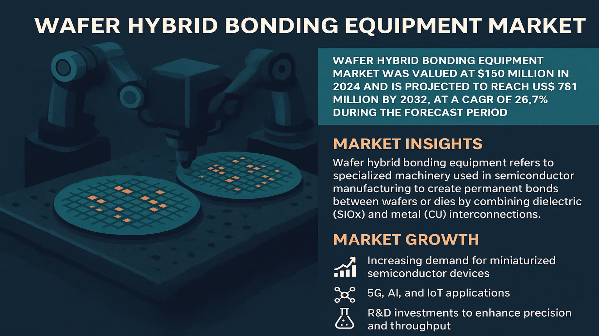
The global Wafer Hybrid Bonding Equipment Market was valued at 150 million in 2024 and is projected to reach US$ 761 million by 2032, at a CAGR of 26.7% during the forecast period.
Wafer hybrid bonding equipment refers to specialized machinery used in semiconductor manufacturing to create permanent bonds between wafers or dies by combining dielectric (SiOx) and metal (Cu) interconnections. This technology enables superior performance compared to traditional through-silicon vias (TSVs) by offering higher I/O density, improved power efficiency, and smaller form factors. The process integrates direct bonding with adhesive techniques to achieve both electrical connectivity and mechanical stability, making it essential for advanced 3D IC packaging, MEMS devices, and high-performance computing applications.
The market growth is driven by increasing demand for miniaturized semiconductor devices, particularly in 5G, AI, and IoT applications. Key players like EV Group and ASMPT are investing in R&D to enhance bonding precision and throughput. However, the high capital expenditure required for equipment remains a barrier for some manufacturers. The CMOS image sensor segment currently dominates application demand, while memory applications like HBM are expected to show significant growth due to their use in data centers and high-performance computing.
MARKET DYNAMICS
MARKET DRIVERS
Growing Demand for 3D ICs and Advanced Packaging Solutions Driving Market Expansion
The global wafer hybrid bonding equipment market is experiencing significant growth due to the semiconductor industry’s increasing adoption of 3D integrated circuits (ICs) and advanced packaging technologies. As chipmakers push beyond the limitations of Moore’s Law, hybrid bonding has emerged as a critical enabler for next-generation semiconductor packaging. The technology allows for vertical stacking of chips with direct copper-to-copper interconnects, delivering superior electrical performance compared to traditional through-silicon vias (TSVs). This is particularly crucial for high-performance computing applications where signal latency and power efficiency are paramount. Recent industry data indicates that 3D IC packaging adoption is growing at an annual rate exceeding 30%, with hybrid bonding solutions accounting for nearly 45% of advanced packaging equipment investments in the semiconductor sector.
Miniaturization Trend in Semiconductor Devices Creating New Demand
As electronic devices continue to shrink in size while demanding greater functionality, the semiconductor industry is increasingly turning to hybrid bonding solutions. This technology enables unprecedented interconnect density, allowing for finer pitch connections below 1μm – a critical requirement for modern CMOS image sensors, memory stacks, and microprocessor units. The precision alignment capabilities of advanced hybrid bonding equipment facilitate this trend, with current-generation systems achieving sub-50nm alignment accuracy for wafer-to-wafer bonding applications. The consumer electronics segment, particularly smartphones and wearables, is driving much of this demand as OEMs seek to pack more functionality into shrinking form factors without compromising performance or battery life.
5G and AI Applications Fueling Adoption in Specialty Semiconductor Markets
The rollout of 5G networks and proliferation of AI applications is creating new opportunities for hybrid bonding technology across various semiconductor segments. High-bandwidth memory (HBM) stacks, essential for AI accelerators and data center GPUs, rely heavily on hybrid bonding for their ultra-dense interconnects. Similarly, RF front-end modules for 5G devices benefit from the technology’s superior signal integrity at millimeter wave frequencies. Major foundries have reported that nearly 60% of their advanced packaging R&D investments are now directed toward hybrid bonding solutions for these high-growth applications. This trend is expected to accelerate as data rates continue climbing and edge computing becomes more pervasive across industries.
MARKET CHALLENGES
High Initial Investment and Operating Costs Limiting Market Penetration
While wafer hybrid bonding technology offers compelling technical advantages, the substantial capital expenditures required for equipment acquisition present a significant barrier to market entry. A complete hybrid bonding production line typically requires investments ranging between $15-25 million, with single tool prices often exceeding $5 million. This places the technology beyond reach for many smaller semiconductor manufacturers and fabless companies. Additionally, the specialized materials and controlled environment requirements add considerable operating expenses, with cleanroom and material costs accounting for approximately 40% of total cost of ownership. These financial constraints are slowing adoption outside the largest semiconductor manufacturers and foundries.
Yield Management Presents Persistent Technical Hurdles
Maintaining high production yields remains one of the most pressing technical challenges in wafer hybrid bonding operations. The bonding process involves multiple critical parameters including surface roughness, cleanliness, temperature uniformity, and alignment precision – all of which must be controlled within extremely tight tolerances. Even nanoscale variations can lead to bonding voids or interconnect failures, with current industry yield rates for complex 3D IC stacks typically ranging between 75-85% for leading-edge applications. This compares unfavorably with the 95%+ yields achievable with conventional packaging methods, creating significant cost pressures for manufacturers implementing hybrid bonding solutions.
Material Compatibility Issues Constraining Design Flexibility
The expansion of hybrid bonding applications is being hindered by material compatibility challenges across different semiconductor technologies. While copper-to-copper bonding has become relatively mature for homogeneous silicon applications, integrating dissimilar materials (such as III-V compounds for photonics or specialty metals for MEMS) often requires complex surface treatments and bonding process modifications. These compatibility issues are particularly problematic for heterogeneous integration scenarios, where thermal expansion mismatches between materials can lead to reliability concerns. Industry data suggests that material-related challenges account for approximately 30% of hybrid bonding development cycles as manufacturers seek to expand the technology’s applicability.
MARKET RESTRAINTS
Shortage of Skilled Personnel Slowing Technology Adoption
The semiconductor industry is facing a critical talent shortage that is particularly acute in advanced packaging domains like hybrid bonding. The specialized knowledge required to operate and maintain hybrid bonding equipment – spanning materials science, precision mechanics, and semiconductor process engineering – is in short supply globally. Surveys indicate that nearly 70% of semiconductor manufacturers report difficulties finding qualified personnel for hybrid bonding operations, with an estimated 40% vacancy rate for these specialized positions. This skills gap is creating bottlenecks in production ramp-ups and limiting the speed at which new hybrid bonding capacity can be brought online.
Immature Supply Chain Creating Implementation Challenges
The hybrid bonding equipment ecosystem is still developing, resulting in supply chain constraints that are slowing market growth. Unlike established semiconductor manufacturing equipment categories, hybrid bonding tools often require custom components with long lead times, while qualified material suppliers remain limited. This has created inventory challenges for equipment manufacturers, with average delivery times extending beyond 9 months for some critical hybrid bonding systems. These supply chain issues are particularly problematic for smaller semiconductor companies that lack the purchasing leverage of larger foundries and IDMs.
Intellectual Property Barriers Restricting Technology Diffusion
The wafer hybrid bonding equipment market faces unique intellectual property challenges that are limiting broader adoption. Core hybrid bonding technologies are protected by dense patent portfolios held by a handful of equipment manufacturers and semiconductor companies. These IP barriers make it difficult for new entrants to develop competitive solutions, while simultaneously forcing companies seeking to implement hybrid bonding into restrictive licensing arrangements. The resulting lack of a robust competitive ecosystem is slowing innovation and keeping prices elevated, with industry estimates suggesting that IP-related costs add approximately 15-20% to total implementation expenses for hybrid bonding solutions.
MARKET OPPORTUNITIES
Emerging Applications in Photonics and Heterogeneous Integration
Hybrid bonding technology is finding new growth opportunities beyond traditional semiconductor applications, particularly in photonics integration and heterogeneous chiplet architectures. The ability to create high-density optical interconnects between silicon photonic devices and electronic ICs is enabling breakthroughs in data center interconnects and telecommunications equipment. Photonic integrated circuit (PIC) manufacturers are increasingly adopting hybrid bonding solutions, with the market for photonics packaging applications projected to grow at over 35% annually. Similarly, the chiplet revolution is creating demand for hybrid bonding equipment capable of integrating disparate semiconductor technologies (logic, memory, analog) into unified packages with high-performance interconnects.
Automotive Sector Presents Significant Growth Potential
The automotive industry’s transition toward electric and autonomous vehicles is creating substantial opportunities for hybrid bonding technology. Advanced driver assistance systems (ADAS) and autonomous driving platforms require high-performance computing solutions that combine multiple sensor inputs with powerful AI processors – an application ideally suited for hybrid bonding’s dense interconnects. Automotive-grade semiconductor packaging must also meet stringent reliability requirements, where hybrid bonding’s superior mechanical strength and thermal performance provide distinct advantages. Industry analysts project that automotive applications will account for over 25% of hybrid bonding equipment demand by 2028, up from less than 10% today.
Equipment Innovation Opening New Market Segments
Recent advancements in hybrid bonding equipment capabilities are expanding the technology’s applicability across new market segments. Next-generation systems capable of room-temperature bonding processes are making the technology accessible to MEMS manufacturers and biomedical device companies. Similarly, the development of more flexible bonding platforms that can accommodate non-standard wafer sizes and materials is unlocking opportunities in specialty semiconductor applications. Equipment vendors report that nearly 40% of recent system sales are going to non-traditional semiconductor customers, signaling a broadening of the market beyond conventional logic and memory applications.
WAFER HYBRID BONDING EQUIPMENT MARKET TRENDS
Increasing Demand for 3D IC Integration to Drive Market Growth
The wafer hybrid bonding equipment market is experiencing substantial growth due to the increasing demand for 3D integrated circuits (3D ICs) in advanced semiconductor packaging. Hybrid bonding, which combines dielectric and metal interconnects, provides superior electrical performance while reducing power consumption compared to traditional methods like through-silicon vias (TSVs). The technology enables vertical stacking of chips, resulting in higher I/O density, improved thermal management, and reduced form factors, making it ideal for applications in high-performance computing (HPC), artificial intelligence (AI), and 5G infrastructure. The market is projected to grow at a compound annual growth rate (CAGR) of 26.7%, with revenue expected to reach $761 million by 2032. The semiconductor industry’s shift toward heterogenous integration and chiplet-based architectures further fuels adoption, as hybrid bonding enhances interconnect reliability in multi-die packages.
Other Trends
Expansion of High-Bandwidth Memory (HBM) Applications
The surge in demand for high-bandwidth memory (HBM) is accelerating the deployment of wafer hybrid bonding technology, particularly in memory-intensive applications like AI accelerators, GPUs, and data centers. HBM leverages hybrid bonding to achieve faster data transfer rates and lower latency while maintaining power efficiency. As AI workloads require increasingly complex neural network models, the need for high-density interconnect solutions has intensified. Leading semiconductor manufacturers are integrating hybrid bonding in next-generation HBM designs, with capacities reaching 24 GB per stack and beyond. This trend is expected to persist as 5G and edge computing applications demand faster, more energy-efficient memory architectures.
Advancements in CMOS Image Sensor (CIS) Packaging
Hybrid bonding equipment is gaining traction in the CMOS image sensor (CIS) segment due to its ability to enhance pixel resolution and light sensitivity in smaller form factors. The technology allows direct bonding of sensor wafers to logic wafers, eliminating the need for microbumps and reducing signal interference. With the growing popularity of high-resolution smartphone cameras, automotive LiDAR systems, and medical imaging devices, manufacturers are investing in hybrid bonding to improve device performance. Recent advancements include backside illuminated (BSI) CIS structures, which further optimize light capture efficiency, driving demand for precision bonding solutions. The automotive sector, in particular, is adopting CIS with hybrid bonding for advanced driver-assistance systems (ADAS), where reliability and miniaturization are critical.
COMPETITIVE LANDSCAPE
Key Industry Players
Technological Innovation Drives Market Leadership in Wafer Hybrid Bonding Equipment
The global wafer hybrid bonding equipment market is characterized by a dynamic competitive environment where both established semiconductor equipment manufacturers and emerging specialists compete for market share. EV Group (EVG) and SUSS MicroTec currently lead the market, owing to their early-mover advantage in advanced packaging solutions and strong partnerships with major foundries. Together, these two players accounted for over 45% of the global market share in 2024, leveraging their expertise in precision alignment and bonding technologies.
ASMPT has been making significant strides in the hybrid bonding segment, particularly in die-to-wafer applications. Their recent acquisition of a bonding technology specialist in 2023 enhanced their capability for high-volume manufacturing solutions. Meanwhile, Piotech and Beijing U-Precision Tech are rapidly gaining traction in the Asian market, supported by government initiatives to strengthen domestic semiconductor supply chains.
The competitive intensity is further heightened by companies expanding their product portfolios through both organic R&D and strategic collaborations. In Q2 2024, EVG introduced its latest generation hybrid bonding system featuring improved throughput and sub-micron alignment accuracy, specifically targeting high-volume memory production. Similarly, SUSS MicroTec partnered with a leading materials supplier to develop optimized process kits for 3D IC applications.
Emerging players like Genesem and Wisdom Semiconductor Technology are focusing on niche applications such as photonics integration and MEMS packaging, differentiating themselves through specialized process knowledge and flexible equipment configurations.
List of Key Wafer Hybrid Bonding Equipment Companies
- EV Group (EVG) (Austria)
- SUSS MicroTec (Germany)
- ASMPT (Singapore)
- Genesem (South Korea)
- C SUN (Taiwan)
- Piotech (China)
- Beijing U-Precision Tech (China)
- Wisdom Semiconductor Technology (China)
Segment Analysis:
By Type
Wafer-to-Wafer Hybrid Bonding Dominates Due to High Throughput in Semiconductor Manufacturing
The market is segmented based on type into:
- Wafer-to-wafer Hybrid Bonding
- Subtypes: Oxide bonding, metal bonding, and others
- Die-to-wafer Hybrid Bonding
- Subtypes: Face-to-face bonding, face-to-back bonding
By Application
CMOS Image Sensors (CIS) Segment Leads Due to Increasing Demand for High-Resolution Cameras
The market is segmented based on application into:
- CMOS Image Sensor (CIS)
- NAND Flash Memory
- DRAM
- High Bandwidth Memory (HBM)
- Others (including MEMS, 3D ICs)
By Technology
Thermo-Compression Bonding Segment Leads Due to Superior Bond Strength in Advanced Packaging
The market is segmented based on technology into:
- Thermo-compression bonding
- Direct bonding
- Oxide fusion bonding
- Adhesive bonding
By End-User
Foundries Segment Leads Due to High Volume Production Requirements
The market is segmented based on end-user into:
- Foundries
- IDMs (Integrated Device Manufacturers)
- OSATs (Outsourced Semiconductor Assembly and Test)
- Research Institutes
Regional Analysis: Wafer Hybrid Bonding Equipment Market
Asia-Pacific
The Asia-Pacific region dominates the global wafer hybrid bonding equipment market, accounting for over 45% of revenue share in 2024. This leadership position stems from concentrated semiconductor manufacturing hubs in Taiwan, South Korea, and mainland China, where major foundries like TSMC, Samsung, and SMIC are actively adopting hybrid bonding technology for advanced packaging. Taiwan alone represents nearly 30% of regional demand, driven by TSMC’s mass production of 3D ICs using hybrid bonding since 2022. Japan also contributes significantly with key equipment suppliers like Tokyo Electron and DISCO developing specialized bonding solutions. While cost sensitivity remains a factor, the push toward 5nm and below nodes is accelerating adoption across the region.
North America
North America’s market growth is fueled by R&D investments in 3D ICs and high-performance computing (HPC), with the U.S. accounting for 80% of regional demand. The CHIPS and Science Act has allocated $52 billion to bolster domestic semiconductor capabilities, including advanced packaging technologies. Major players like Intel and GlobalFoundries are expanding hybrid bonding applications for AI/ML chips and data center processors. Academic collaborations, such as those with IMEC and SEMATECH, further drive innovation. However, high equipment costs and a reliance on Asian foundries for mass production temper near-term growth.
Europe
Europe’s market centers on specialized applications in automotive and photonics, with Germany, France, and the Netherlands as key adopters. The region benefits from strong MEMS and sensor industries, where hybrid bonding enhances performance in automotive LiDAR and medical devices. EU-funded initiatives like the Key Digital Technologies partnership support equipment development, though fragmentation across SMEs limits economies of scale. ASML and Besi are among the few European equipment manufacturers competing globally, focusing on precision alignment technologies crucial for hybrid bonding.
Middle East & Africa
This emerging market shows potential through strategic partnerships, such as Saudi Arabia’s $6 billion investment in semiconductor packaging under Vision 2030. Israel’s Tower Semiconductor also contributes to niche demand for RF and MEMS applications. However, limited local fabrication capacity and reliance on imported equipment constrain growth. The UAE’s Dubai Silicon Oasis represents one of the few infrastructure projects with wafer-level packaging capabilities in the region.
South America
South America remains a minor player, with Brazil’s CEITEC being the sole domestic wafer fab. Most demand comes from consumer electronics assembly in Mexico and testing facilities in Brazil. Economic instability and lack of government incentives hinder capital-intensive equipment purchases, though some multinationals use the region for legacy packaging operations. Growth hinges on attracting foreign investment in advanced packaging clusters.
Report Scope
This market research report provides a comprehensive analysis of the Global Wafer Hybrid Bonding Equipment Market, covering the forecast period 2025–2032. It offers detailed insights into market dynamics, technological advancements, competitive landscape, and key trends shaping the semiconductor equipment industry.
Key focus areas of the report include:
- Market Size & Forecast: Historical data and future projections for revenue, unit shipments, and market value across major regions and segments. The market was valued at USD 150 million in 2024 and is projected to reach USD 761 million by 2032, growing at a CAGR of 26.7%.
- Segmentation Analysis: Detailed breakdown by bonding type (wafer-to-wafer and die-to-wafer), application (CIS, NAND, DRAM, HBM), and end-use industries to identify high-growth segments and investment opportunities.
- Regional Outlook: Insights into market performance across North America, Europe, Asia-Pacific, Latin America, and Middle East & Africa, with country-level analysis of key semiconductor manufacturing hubs.
- Competitive Landscape: Profiles of leading market participants including EV Group, SUSS MicroTec, ASMPT, and emerging players, covering their product portfolios, technological capabilities, and strategic initiatives.
- Technology Trends & Innovation: Assessment of emerging bonding techniques, integration with advanced packaging solutions, and the impact of AI/ML in wafer bonding processes.
- Market Drivers & Restraints: Evaluation of factors such as 3D IC adoption, automotive electronics growth, and challenges like high capital expenditure and process complexity.
- Stakeholder Analysis: Strategic insights for semiconductor equipment manufacturers, foundries, IDMs, OSATs, and investors regarding technology adoption and market opportunities.
The research employs primary interviews with industry experts and analysis of verified market data to ensure accuracy and reliability of insights.
FREQUENTLY ASKED QUESTIONS:
What is the current market size of Global Wafer Hybrid Bonding Equipment Market?
-> Wafer Hybrid Bonding Equipment Market was valued at 150 million in 2024 and is projected to reach US$ 761 million by 2032, at a CAGR of 26.7% s.
Which key companies operate in this market?
-> Key players include EV Group (EVG), SUSS MicroTec, ASMPT, Piotech, and Beijing U-Precision Tech, with emerging competitors gaining market share.
What are the key growth drivers?
-> Primary drivers include rising demand for 3D ICs, advanced packaging solutions, and growth in automotive electronics and 5G applications.
Which region dominates the market?
-> Asia-Pacific leads the market due to semiconductor manufacturing concentration, while North America shows strong growth in R&D and advanced packaging.
What are the emerging trends?
-> Emerging trends include sub-micron alignment precision, integration with wafer-level packaging, and development of heterogeneous integration solutions.

Get Sample Report PDF for Exclusive Insights
Report Sample Includes
- Table of Contents
- List of Tables & Figures
- Charts, Research Methodology, and more...
 Download Sample Report PDF