
Market Insights
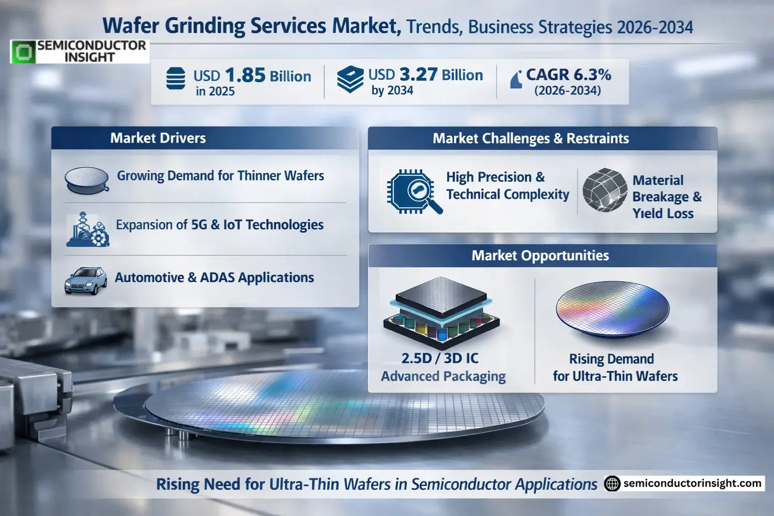
Global Wafer Grinding Services Market size was valued at USD 1.85 billion in 2025. The market is projected to grow from USD 2.02 billion in 2026 to USD 3.27 billion by 2034, exhibiting a CAGR of 6.3% during the forecast period.
Wafer grinding services involve precision thinning of semiconductor wafers to achieve desired thickness and surface quality, critical for advanced chip manufacturing. These services utilize specialized equipment such as grinders, polishers, and metrology tools to ensure uniformity and minimize defects in wafers used across industries like consumer electronics, automotive, and data centers.
The market growth is driven by increasing demand for thinner wafers in compact electronic devices and the rapid expansion of the semiconductor industry. Key players like DISCO Corporation and AXUS TECHNOLOGY are investing in advanced grinding technologies to enhance efficiency and meet stringent industry standards. Additionally, rising adoption of ultra-thin wafers in IoT and AI applications further fuels market expansion.
MARKET DRIVERS
Growing Demand for Thinner Semiconductor Wafers
Wafer Grinding Services Market is experiencing significant growth due to the rising demand for thinner semiconductor wafers in advanced electronics. Thinner wafers enable higher performance and energy efficiency in devices, driving manufacturers to seek precision grinding solutions. The market has grown by approximately 12% annually as chip manufacturers push the boundaries of miniaturization.
Expansion of 5G and IoT Technologies
Emerging technologies like 5G networks and IoT devices require specialized semiconductor components, creating new opportunities for wafer grinding services. The need for high-frequency chips with precise thickness control has increased demand by over 15% in the past two years, particularly in Asia-Pacific markets.
Automotive electrification and advanced driver-assistance systems (ADAS) are additional growth factors, as these applications require durable, high-performance semiconductor components with exact thickness specifications.
MARKET CHALLENGES
High Precision Requirements and Technical Complexity
Wafer grinding services face significant technical challenges as semiconductor manufacturers demand sub-micron level precision. Achieving consistent results across large production volumes remains difficult, with yield rates varying between 85-93% depending on wafer material and thickness requirements.
Other Challenges
Equipment Costs and Maintenance
Advanced wafer grinding systems require multi-million dollar investments, with annual maintenance costs consuming 15-20% of the initial capital expenditure. This creates barriers to entry for smaller service providers.
MARKET RESTRAINTS
Material Breakage and Yield Loss Concerns
Wafer Grinding Services Market faces constraints from material breakage during the thinning process, particularly with ultra-thin wafers below 50μm. Even with advanced handling techniques, breakage rates of 3-5% can significantly impact production costs and timelines. Some manufacturers are exploring alternative thinning technologies as a result.
MARKET OPPORTUNITIES
Emerging Advanced Packaging Technologies
Wafer Grinding Services Market stands to benefit from growing adoption of 2.5D and 3D IC packaging solutions, which require precise wafer thinning and dicing. Market analysts project a 20% CAGR for these advanced packaging applications through 2027, with wafer grinding services being a critical enabling technology.
Wafer Grinding Services Market Trends
Increasing Demand for Ultra-Thin Wafers in Semiconductor Applications
Wafer Grinding Services Market is experiencing significant growth driven by rising demand for ultra-thin wafers in advanced semiconductor packaging. As chip manufacturers push for higher performance in smaller form factors, the need for precision thinning of silicon wafers continues to grow across consumer electronics, automotive, and data center applications.
Other Trends
Technological Advancements in Grinding Equipment
Leading companies like DISCO Corporation and AXUS TECHNOLOGY are investing in next-generation grinding systems with improved precision and automation capabilities. These advancements enable thinner wafer processing while maintaining structural integrity, addressing key challenges in semiconductor manufacturing.
Regional Market Expansion in Asia-Pacific
The Asia-Pacific region continues to dominate the Wafer Grinding Services Market, with China, Japan, and South Korea representing key growth areas. This expansion is fueled by the concentration of semiconductor fabrication facilities and increased investments in domestic manufacturing capabilities across these countries.
Growing Adoption in Automotive Electronics
The automotive sector is emerging as a significant consumer of wafer grinding services, particularly for advanced driver assistance systems (ADAS) and vehicle electrification components. This trend is expected to accelerate as automotive semiconductor content continues to increase annually.
Industry Consolidation and Strategic Partnerships
The market has witnessed several strategic collaborations between wafer grinding service providers and semiconductor manufacturers. Companies like Silicon Valley Microelectronics and Phoenix Silicon International are forming alliances to enhance their service offerings and expand their geographic reach in this competitive landscape.
COMPETITIVE LANDSCAPE
Key Industry Players
Wafer Grinding Services Market Dominated by Specialized Providers and Semiconductor Giants
Wafer Grinding Services Market features a mix of specialized semiconductor service providers and established equipment manufacturers. DISCO Corporation leads the industry with advanced grinding technologies and global service networks, capturing significant market share. Other major players like AXUS TECHNOLOGY and SIEGERT WAFER GmbH maintain strong positions through precision grinding capabilities for ultra-thin wafers used in advanced packaging applications.
Several regional players such as NICHIWA KOGYO CO.,LTD. in Japan and Phoenix Silicon International in Taiwan cater to local semiconductor manufacturing ecosystems. Emerging players like Aptek Industries are gaining traction through innovative grinding solutions for compound semiconductor materials. The competitive landscape remains dynamic with increasing demand for wafer thinning services from automotive electronics and data center applications.
List of Key Wafer Grinding Services Companies Profiled
- Syagrus Systems
- Optim Wafer Services
- Silicon Valley Microelectronics, Inc.
- SIEGERT WAFER GmbH
- NICHIWA KOGYO CO.,LTD.
- Integra Technologies
- Valley Design
- AXUS TECHNOLOGY
- Helia Photonics
- DISCO Corporation
- Aptek Industries
- UniversityWafer, Inc.
- Enzan Factory Co., Ltd.
- Phoenix Silicon International
- Prosperity Power Technology Inc.
Segment Analysis:
| Segment Category | Sub-Segments | Key Insights |
| By Type |
|
Ultra-Thin Wafers segment shows strongest growth potential due to:
|
| By Application |
|
Automotive Electronics emerges as most promising sector owing to:
|
| By End User |
|
Foundries represent key customers due to:
|
| By Technology |
|
Chemical-Mechanical Polishing (CMP) dominates technology segment because:
|
| By Wafer Size |
|
300mm Wafers remain primary focus because:
|
Regional Analysis: Global Wafer Grinding Services Market
Asia-Pacific
Japan maintains technological supremacy with advanced grinding equipment and specialized processes for delicate wafers. The region pioneers ultra-thin wafer handling solutions achieving <100μm thickness while minimizing breakage – critical for 3D IC packaging applications. Taiwanese and South Korean providers excel in high-throughput grinding for volume production.
The region hosts complete wafer processing ecosystems from silicon wafer suppliers to OSAT providers. Clusters like Taiwan’s Hsinchu Science Park create efficient workflows where grinding services are tightly integrated with upstream wafer production and downstream packaging operations, reducing logistics costs and turnaround times.
Substantial government investments across the region boost wafer grinding capabilities. China’s semiconductor self-sufficiency drive allocates billions to advanced packaging infrastructure, while South Korea’s semiconductor cluster expansion plans include dedicated wafer thinning R&D centers. Japan funds next-generation grinding technology development through METI initiatives.
Growing adoption of advanced packaging in automotive and AI chips drives demand for specialized wafer grinding services across the region. Providers are developing unique solutions for power devices, MEMS sensors, and RF applications requiring precise thickness control and stress management during grinding processes.
North America
North America maintains strong wafer grinding capabilities through specialized providers serving aerospace, defense and high-performance computing sectors. The region benefits from close university-industry collaborations developing novel grinding techniques and materials. California’s semiconductor cluster hosts several advanced wafer thinning R&D centers working on next-generation solutions for heterogeneous integration. While production volumes trail Asia, North American providers excel in high-mix, low-volume prototyping and specialized military/aerospace applications requiring ITAR-compliant processing. The region sees growing investment in wafer-level grinding for photonics and compound semiconductor devices.
Europe
Europe’s wafer grinding market is characterized by strong automotive semiconductor demand and MEMS applications. Germany leads with precision engineering expertise applied to automotive power devices and sensors. The region benefits from a concentration of specialty equipment manufacturers developing advanced grinding machines. Collaborative R&D projects through programs like Horizon Europe foster development of environmentally sustainable grinding processes. While trailing Asia in production scale, European providers maintain leadership in customized grinding solutions for niche applications like medical devices and industrial sensors requiring ultra-clean processing environments.
South America
South America’s emerging wafer grinding capabilities primarily serve local consumer electronics and automotive manufacturing. Brazil leads regional development with growing investments in semiconductor back-end processing infrastructure. The market remains in early stages, focusing on basic grinding services for legacy nodes. Limited local wafer production necessitates reliance on imported blanks, increasing processing costs. However, proximity to North American markets provides potential for nearshoring opportunities as regional semiconductor policies evolve to attract more back-end investment.
Middle East & Africa
The Middle East is making strategic investments in semiconductor manufacturing, with wafer grinding services emerging as part of broader technology diversification efforts. Saudi Arabia’s semiconductor strategy includes plans for advanced packaging facilities requiring grinding capabilities. Africa presents limited current capacity but shows potential for basic grinding services to support nascent electronics manufacturing ecosystems in North Africa. Both regions face challenges in establishing complete supply chains and technical workforces for wafer processing.
Report Scope
This market research report provides a comprehensive analysis of the Wafer Grinding Services Market, covering the forecast period 2025–2034. It offers detailed insights into market dynamics, technological advancements, competitive landscape, and key trends shaping the industry.
Key focus areas of the report include:
- Market Overview: The report begins with an overview outlining its current market scenario, key growth indicators, and industry transformation drivers. It discusses macroeconomic factors, demand–supply balance, regulatory landscape, and the strategic role of semiconductors in powering advancements across industries such as consumer electronics, automotive electronics, computer/data centers, and industrial automation.
- Market Size & Forecast: Historical data and future projections for revenue, unit shipments, and market value across major regions and segments.
- Segmentation Analysis: Detailed breakdown by product type, including Ordinary Wafers and Ultra-Thin Wafers, as well as application segments like Consumer Electronics, Automotive Electronics, Computer and Data Center, and others.
- Regional Insights: Insights into market performance across North America, Europe, Asia, South America, and Middle East & Africa, including country-level analysis for key markets like U.S., China, Japan, and Germany.
- Competitive Landscape: Profiles of leading market participants, including their product offerings, manufacturing capacity, pricing strategies, and recent developments.
- Technology Trends & Innovation: Assessment of emerging wafer grinding technologies, fabrication techniques, and evolving industry standards.
- Market Drivers & Restraints: Evaluation of factors driving market growth along with challenges, supply chain constraints, and regulatory issues.
- Stakeholder Insights: Strategic opportunities for semiconductor manufacturers, equipment suppliers, and investors in the wafer grinding ecosystem.
Primary and secondary research methods are employed, including interviews with industry experts and data from verified sources to ensure the accuracy and reliability of the insights presented.
FREQUENTLY ASKED QUESTIONS:
What is the current market size of Wafer Grinding Services Market?
-> Wafer Grinding Services Market size was valued at USD 1.85 billion in 2025. The market is projected to grow from USD 2.02 billion in 2026 to USD 3.27 billion by 2034, exhibiting a CAGR of 6.3% during the forecast period.
Which key companies operate in Wafer Grinding Services Market?
-> Key players include Syagrus Systems, Optim Wafer Services, Silicon Valley Microelectronics, SIEGERT WAFER GmbH, NICHIWA KOGYO CO.,LTD., Integra Technologies, Valley Design, AXUS TECHNOLOGY, Helia Photonics, and DISCO Corporation, among others. The top five players accounted for approximately % of global revenue in 2025.
What are the key growth drivers?
-> Key growth drivers include increasing demand for consumer electronics, growth in automotive electronics, expansion of data centers, and technological advancements in semiconductor manufacturing.
Which application segment dominates the market?
-> Consumer Electronics currently holds the largest market share, while Automotive Electronics and Computer/Data Center applications are showing the fastest growth rates.
Which region has the highest market share?
-> Asia dominates the Global Wafer Grinding Services Market, with significant contributions from China, Japan, and South Korea. The U.S. market is estimated at USD million in 2025.
Get Sample Report PDF for Exclusive Insights
Report Sample Includes
- Table of Contents
- List of Tables & Figures
- Charts, Research Methodology, and more...
 Download Sample Report PDF





