
Wafer Frontside Metallization Service Market Insights
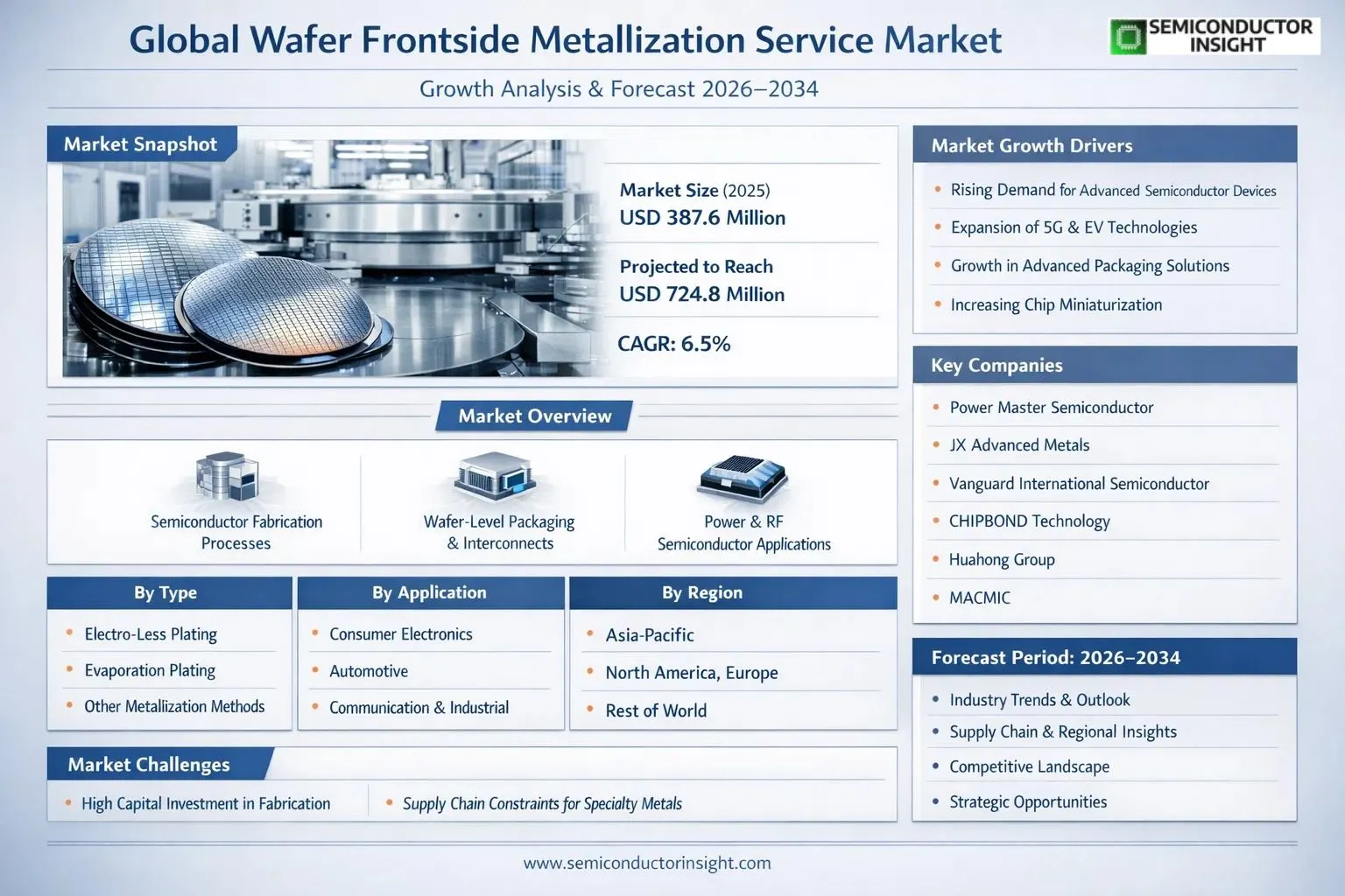
Global Wafer Frontside Metallization Service market size was valued at USD 387.6 million in 2025. The market is projected to grow from USD 412.4 million in 2026 to USD 724.8 million by 2034, exhibiting a CAGR of 6.5% during the forecast period.
Wafer Frontside Metallization Service is a semiconductor manufacturing service primarily focused on depositing metal layers on the front surface of wafers. This process is critical for circuit interconnections and product performance, typically employing techniques such as evaporation, sputtering, or chemical vapor deposition to ensure conductivity and mechanical integrity. The service encompasses key process types including Electro-Less Plating, Evaporation Plating, and other advanced deposition methodologies.
The market is witnessing sustained momentum driven by the accelerating global demand for semiconductors across consumer electronics, automotive, and industrial applications. The proliferation of advanced packaging technologies and the ongoing miniaturization of integrated circuits are further intensifying the need for precise frontside metallization capabilities. Key players operating in Global market include Power Master Semiconductor Co., Ltd., JX Advanced Metals Corporation, Vanguard International Semiconductor Corporation, Axetris, Prosperity Power Technology Inc., Integrated Service Technology Inc., CHIPBOND Technology Corporation, Huahong Group, and MACMIC, among others, each maintaining competitive portfolios to address diverse end-use requirements across multiple geographies.
MARKET DRIVERS
Rising Demand for Advanced Semiconductor Packaging Fuels Growth in Wafer Frontside Metallization Service Market
Wafer Frontside Metallization Service Market is experiencing significant momentum driven by the accelerating global demand for advanced semiconductor devices. As integrated circuit designs become increasingly complex, the need for precise and reliable frontside metallization processes , including physical vapor deposition (PVD), chemical vapor deposition (CVD), and electroplating techniques , has grown substantially. Semiconductor manufacturers are investing heavily in outsourced metallization services to achieve tighter process tolerances and superior electrical conductivity in device interconnects, which is a critical performance parameter in high-frequency and power electronics applications.
Proliferation of 5G Infrastructure and Electric Vehicles Creating Sustained Demand
Global rollout of 5G telecommunications infrastructure and the rapid adoption of electric vehicles (EVs) are generating strong downstream demand for power semiconductors, RF chips, and high-density ICs , all of which require sophisticated frontside metallization processes. Power devices used in EV inverters and chargers, for example, rely on robust metal contact layers to handle high current densities without degradation. This has made Wafer Frontside Metallization Service Market a critical enabler of the broader semiconductor supply chain, with foundries and integrated device manufacturers (IDMs) increasingly relying on specialized service providers to manage metallization complexity.
➤ The convergence of miniaturization trends and heterogeneous integration strategies is compelling semiconductor manufacturers to adopt outsourced wafer frontside metallization services, positioning specialist providers as indispensable partners in the advanced chip fabrication ecosystem.
Advances in wafer-level packaging (WLP) and fan-out packaging technologies are further propelling the market. These packaging architectures depend critically on high-precision metal deposition on the wafer frontside to form reliable redistribution layers (RDLs) and under-bump metallization (UBM) structures. As packaging density requirements intensify alongside shrinking node geometries, the technical expertise and capital equipment intensity involved in frontside metallization are increasingly driving semiconductor companies to partner with dedicated service providers rather than managing the process in-house.
MARKET CHALLENGES
High Capital Expenditure and Process Complexity Pose Significant Barriers for Wafer Frontside Metallization Service Providers
One of the foremost challenges confronting participants in Wafer Frontside Metallization Service Market is the substantial capital investment required to establish and maintain state-of-the-art metallization infrastructure. Advanced deposition systems, lithography tools for metal patterning, and sophisticated process control equipment collectively represent multi-million-dollar investments. Smaller service providers often face difficulties in keeping pace with the rapid evolution of process requirements driven by leading-edge node development, creating a bifurcation in the competitive landscape between well-capitalized incumbents and emerging regional players.
Other Challenges
Supply Chain Vulnerabilities for Specialty Metals and Process Gases
Wafer Frontside Metallization Service Market is exposed to supply chain risks associated with specialty raw materials, including high-purity targets for sputtering (such as tungsten, titanium, and aluminum alloys) and ultra-pure process gases. Geopolitical disruptions, export controls, and concentration of supply among a limited number of global producers have periodically introduced material cost volatility and availability constraints, complicating production planning for metallization service providers.
Stringent Quality and Contamination Control Requirements
Frontside metallization processes demand exceptionally low contamination thresholds to preserve device yield and reliability. Managing particle counts, metallic contamination, and film uniformity across large-diameter wafers (300mm and beyond) remains technically demanding. Service providers must continuously invest in cleanroom upgrades, advanced metrology systems, and rigorous process qualification protocols to meet the exacting standards set by leading semiconductor customers, adding to operational cost pressures.
MARKET RESTRAINTS
Geopolitical Tensions and Export Regulations Constraining Market Expansion in Key Regions
Wafer Frontside Metallization Service Market faces meaningful restraints arising from the intensifying geopolitical landscape surrounding semiconductor technology. Export control regulations imposed by major economies on advanced semiconductor manufacturing equipment and materials have created uncertainty for service providers operating across international supply chains. Restrictions on technology transfer and equipment procurement have in certain cases delayed capacity expansion programs, particularly among providers seeking to upgrade to processes compatible with sub-28nm technology nodes, thereby moderating the pace of market growth in affected geographies.
Transition to Alternative Interconnect Materials Introducing Process Transition Risk
The semiconductor industry’s gradual evaluation of alternative interconnect and contact materials , such as ruthenium and cobalt as replacements for conventional tungsten and aluminum in advanced nodes , introduces a degree of process transition risk for established Wafer Frontside Metallization Service providers. Companies that have made significant investments in legacy process platforms may face margin compression and capital write-down risks as customer roadmaps evolve. This technological transition dynamic acts as a near-term restraint, requiring service providers to continuously reallocate R&D resources and capital to remain aligned with leading-edge process requirements, which can strain profitability particularly for mid-tier operators.
MARKET OPPORTUNITIES
Expanding Semiconductor Fab Investments Across Asia-Pacific and North America Opening New Service Opportunities
Government-backed semiconductor manufacturing incentive programs in the United States, Europe, Japan, South Korea, and India are catalyzing a new wave of wafer fabrication facility construction, representing a substantial growth opportunity for Wafer Frontside Metallization Service Market. As greenfield and brownfield fabs come online over the coming years, demand for qualified metallization service partners with demonstrated process expertise is expected to increase materially. Service providers that proactively establish regional partnerships and co-locate capabilities near emerging fab clusters stand to capture significant incremental revenue as these facilities ramp to full production capacity.
Growth in Wide Bandgap Semiconductor Devices Creating a New Frontier for Metallization Services
The accelerating commercialization of silicon carbide (SiC) and gallium nitride (GaN) power devices presents a compelling adjacent opportunity for Wafer Frontside Metallization Service Market. Wide bandgap semiconductors require specialized ohmic contact metallization schemes that differ meaningfully from conventional silicon processes, necessitating distinct process development and qualification investments. Service providers capable of developing and offering certified metallization solutions tailored to SiC and GaN device architectures are well-positioned to differentiate their offerings and command premium pricing, particularly given the strong growth trajectory of these materials in EV powertrains, renewable energy inverters, and industrial motor drives.
Outsourcing Trend Among Fabless and Fab-Lite Companies Driving Structural Market Expansion
The continued expansion of the fabless semiconductor design ecosystem and the growing preference among fab-lite companies for outsourcing capital-intensive back-end-of-line (BEOL) and metallization processes represent a durable structural driver for Wafer Frontside Metallization Service Market. As design companies seek to minimize fixed asset exposure while accessing world-class process technology, specialist metallization service providers that offer flexible capacity, rapid process qualification turnaround, and competitive yield guarantees are increasingly favored. This outsourcing dynamic is expected to broaden the addressable customer base for dedicated frontside metallization service providers, supporting sustained market expansion over the medium to long term.
Wafer Frontside Metallization Service Market Trends
Rising Demand from Advanced Semiconductor Packaging Driving Wafer Frontside Metallization Service Market
Wafer Frontside Metallization Service Market is experiencing notable momentum driven by increasing demand for high-performance semiconductor components across multiple end-use industries. As integrated circuit designs grow more complex, the need for precise and reliable front-surface metal deposition has become more critical than ever. Metallization techniques such as sputtering, evaporation, and electro-less plating are being refined to meet tighter design tolerances, especially as device miniaturization continues to accelerate. The automotive and consumer electronics sectors, in particular, are placing greater emphasis on wafer-level performance, pushing service providers to continuously enhance deposition uniformity and adhesion quality across diverse substrate materials.
Other Trends
Expansion of Electro-Less Plating Applications
Electro-less plating is emerging as one of the most technically favored processes within Wafer Frontside Metallization Service Market. Unlike conventional electroplating, electro-less plating offers uniform metal deposition across complex geometries without requiring an external electrical current, making it highly suitable for advanced node wafer processing. Service providers are investing in process optimization to improve the repeatability and purity of deposited layers, especially for applications in communication chips and industrial sensors. This segment is anticipated to witness sustained adoption as device architects continue to prioritize conformal metal coverage at finer feature dimensions.
Growing Influence of the Automotive Semiconductor Segment
The automotive industry’s rapid transition toward electrification and advanced driver-assistance systems (ADAS) is creating significant new demand within Wafer Frontside Metallization Service Market. Power semiconductors, radar chips, and sensor components used in modern vehicles require high-integrity frontside metallization to ensure long-term operational reliability under demanding thermal and mechanical conditions. Service providers are aligning their metallization capabilities to address automotive-grade quality standards, including stringent requirements for metal layer thickness consistency, resistivity control, and resistance to environmental stress. This trend is expected to remain a key growth catalyst as vehicle electrification accelerates globally.
Asia-Pacific Consolidating Its Role as a Core Service Hub
Asia-Pacific continues to reinforce its position as the dominant regional hub for wafer fabrication and associated services, including frontside metallization. Countries such as China, South Korea, Japan, and Taiwan host a dense ecosystem of semiconductor foundries and outsourced semiconductor assembly and test (OSAT) facilities that rely on high-quality metallization services. Leading market participants, including Power Master Semiconductor Co., Ltd., Vanguard International Semiconductor Corporation, CHIPBOND Technology Corporation, and Huahong Group, are actively scaling their service capacities in this region to address growing order volumes. Strategic collaborations between metallization service providers and wafer foundries are becoming more common as the industry works to streamline supply chain integration and reduce turnaround times, further strengthening the competitive landscape of Wafer Frontside Metallization Service Market.
COMPETITIVE LANDSCAPE
Key Industry Players
Wafer Frontside Metallization Service Market , Competitive Dynamics, Leading Manufacturers, and Strategic Positioning
Global Wafer Frontside Metallization Service market is characterized by a moderately consolidated competitive landscape, where a handful of established semiconductor foundries and specialized metallization service providers command significant revenue share. Power Master Semiconductor Co., Ltd. and JX Advanced Metals Corporation are among the most prominent players, leveraging advanced deposition technologies , including sputtering, evaporation plating, and electro-less plating , to serve a diverse customer base spanning consumer electronics, automotive electronics, industrial applications, and communication infrastructure. Vanguard International Semiconductor Corporation has also emerged as a formidable competitor, capitalizing on its broad wafer processing capabilities and deep integration across front-end semiconductor manufacturing workflows. As of 2025, the top five global players collectively account for a notable share of overall market revenue, underscoring the degree of concentration at the upper tier of this industry. These leading companies continue to invest in capacity expansion, process innovation, and strategic partnerships to strengthen their foothold in key regional markets, particularly in Asia-Pacific, which remains the dominant hub for wafer metallization services.
Beyond the top-tier players, Wafer Frontside Metallization Service Market also features a range of specialized niche participants that contribute to technology diversification and regional supply chain resilience. CHIPBOND Technology Corporation and Huahong Group have established strong presences in East Asian markets, offering cost-competitive metallization solutions tailored to high-volume production environments. Integrated Service Technology Inc. and Prosperity Power Technology Inc. cater to precision-focused segments, providing customized metallization processes for power semiconductors and MEMS devices. Axetris, with its expertise in microfabrication and thin-film deposition, addresses niche industrial and sensor-related applications requiring high-precision frontside metal layer integrity. MACMIC rounds out the competitive field with its growing portfolio of metallization services targeting mid-tier semiconductor manufacturers across Asia. The competitive intensity within this market is further amplified by the ongoing shift toward electro-less plating techniques, which offer superior conformality and cost efficiency, prompting both established players and emerging entrants to accelerate R&D investments and service diversification strategies.
List of Key Wafer Frontside Metallization Service Companies Profiled
- Power Master Semiconductor Co., Ltd.
- JX Advanced Metals Corporation
- Vanguard International Semiconductor Corporation
- Axetris
- Prosperity Power Technology Inc.
- Integrated Service Technology Inc.
- CHIPBOND Technology Corporation
- Huahong Group
- MACMIC
- Advanced Semiconductor Engineering (ASE Group)
- Amkor Technology
- UTAC Holdings
- Tongfu Microelectronics Co., Ltd.
- King Yuan Electronics Co., Ltd. (KYEC)
- Chipmos Technologies Inc.
Segment Analysis:
| Segment Category | Sub-Segments | Key Insights |
| By Type |
|
Electro-Less Plating holds a prominent position in Wafer Frontside Metallization Service Market owing to its ability to deposit uniform metal layers without the need for an external electrical current, making it highly suitable for complex and intricate wafer geometries.
|
| By Application |
|
Consumer Electronics represents the leading application segment in Wafer Frontside Metallization Service Market, driven by the perpetual demand for smaller, faster, and more power-efficient semiconductor devices embedded in smartphones, tablets, wearables, and smart home systems.
|
| By End User |
|
Fabless Semiconductor Companies emerge as the dominant end-user segment in Wafer Frontside Metallization Service Market, as these organizations rely entirely on third-party foundry and specialty service providers for all aspects of wafer fabrication and processing, including frontside metallization.
|
| By Deposition Technology |
|
Physical Vapor Deposition (PVD) / Sputtering stands as the leading deposition technology segment, widely regarded as the industry workhorse for wafer frontside metallization due to its versatility, cost-effectiveness, and compatibility with a broad range of metal materials including aluminum, titanium, and copper.
|
| By Wafer Size |
|
300mm (12-inch) Wafers represent the dominant wafer size segment within Wafer Frontside Metallization Service Market, reflecting the broader semiconductor industry’s migration toward larger wafer formats to achieve higher throughput and improved economies of scale in device manufacturing.
|
Regional Analysis: Wafer Frontside Metallization Service Market
Asia-Pacific
Asia-Pacific hosts a dense network of advanced semiconductor fabs, many of which are equipped with cutting-edge metallization equipment capable of handling sub-5nm node wafers. This infrastructure advantage ensures that wafer frontside metallization service providers in the region operate at scale and with unmatched process precision, meeting both high-volume and specialty application demands across diverse end-use industries.
Strategic national policies across China, Japan, South Korea, and India are accelerating investments in domestic semiconductor value chains. Subsidies, tax incentives, and dedicated semiconductor development programs are enabling local wafer frontside metallization service providers to upgrade process capabilities, reduce dependency on foreign technology, and compete more effectively in Global market landscape through 2034.
The explosive growth of consumer electronics, electric vehicles, 5G infrastructure, and artificial intelligence accelerators across Asia-Pacific directly fuels demand for precise frontside metallization services. These application segments require flawless metal contact formation on wafer surfaces, making high-quality metallization services indispensable to regional chip manufacturers aiming for improved yield and device reliability at advanced technology nodes.
Asia-Pacific is home to prolific semiconductor research institutions and corporate R&D centers focused on developing next-generation metallization materials and deposition techniques. Innovations in barrier layer engineering, low-resistivity metal integration, and atomic-layer deposition processes are advancing the quality and performance of wafer frontside metallization services, reinforcing the region’s technological leadership in global semiconductor manufacturing ecosystems.
North America
North America represents a strategically vital region in Wafer Frontside Metallization Service Market, anchored by the United States’ robust semiconductor design ecosystem and its growing emphasis on domestic fabrication capacity. Landmark legislative frameworks aimed at revitalizing onshore chip production are prompting substantial capital flows into new and expanded wafer processing facilities, which in turn elevate the demand for specialized frontside metallization services. The region is home to several leading semiconductor companies and research universities that continuously push the boundaries of metallization process innovation. Demand from high-performance computing, defense electronics, aerospace, and advanced medical devices further strengthens North America’s position in Global Wafer Frontside Metallization Service Market. As regional foundry capacity expands through the forecast period, metallization service providers are expected to scale operations accordingly to support domestic chip manufacturing ambitions.
Europe
Europe holds a meaningful and growing position in Wafer Frontside Metallization Service Market, supported by a strong tradition of precision engineering and a targeted policy focus on semiconductor sovereignty. The European Chips Act has galvanized investment in wafer fabrication and associated specialty services, including frontside metallization, across Germany, the Netherlands, France, and other key member states. European semiconductor manufacturers are increasingly prioritizing the localization of critical process steps, reducing reliance on external service providers for high-sensitivity metallization work. The region’s expertise in automotive-grade semiconductors, industrial electronics, and power devices creates consistent demand for reliable and high-quality wafer frontside metallization services. Innovation in wide-bandgap semiconductor materials further opens new metallization process requirements unique to the European market.
South America
South America remains an emerging participant in Wafer Frontside Metallization Service Market, with its semiconductor ecosystem still in the early stages of formalized development. Brazil leads regional activity, supported by nascent government programs aimed at building foundational semiconductor infrastructure. While the region does not yet operate large-scale wafer metallization service facilities, growing demand for electronics assembly and increasing foreign direct investment in technology sectors are slowly creating a foundation for future growth. Regional players are beginning to explore partnerships with established global metallization service providers to gain technical knowledge and process capabilities. Over the long forecast horizon of 2026–2034, South America may progressively develop more structured participation in Wafer Frontside Metallization Service Market, particularly as global supply chain diversification trends gain momentum.
Middle East & Africa
The Middle East and Africa region currently occupies a nascent but strategically noteworthy position in Wafer Frontside Metallization Service Market. Gulf Cooperation Council nations, particularly the United Arab Emirates and Saudi Arabia, are channeling substantial investment into technology infrastructure as part of broader economic diversification strategies. While indigenous wafer metallization service capacity is limited at present, the region’s ambition to develop knowledge-based economies is gradually attracting semiconductor technology partnerships and talent development programs. Africa’s expanding digital economy and growing electronics consumption base represent long-term demand catalysts. As global semiconductor companies seek geographic diversification in their service networks, the Middle East and Africa may emerge as an incremental contributor to Wafer Frontside Metallization Service Market landscape through the latter years of the 2026–2034 forecast period.
Report Scope
This market research report provides a comprehensive analysis of Wafer Frontside Metallization Service Market, covering the forecast period 2026–2034. It offers detailed insights into market dynamics, technological advancements, competitive landscape, and key trends shaping the industry.
Key focus areas of the report include:
- Market Overview: The report begins with an overview outlining its current market scenario, key growth indicators, and industry transformation drivers. It discusses macroeconomic factors, demand–supply balance, regulatory landscape, and the strategic role of semiconductors in powering advancements across industries such as automotive, telecommunications, consumer electronics, and industrial automation.
- Market Size & Forecast: Historical data and future projections for revenue, unit shipments, and market value across major regions and segments.
- Segmentation Analysis: Detailed breakdown by product type, technology, application, and end-user industry to identify high-growth segments and investment opportunities.
- Regional Insights: Insights into market performance across North America, Europe, Asia-Pacific, Latin America, and the Middle East & Africa, including country-level analysis where relevant.
- Competitive Landscape: Profiles of leading market participants, including their product offerings, R&D focus, manufacturing capacity, pricing strategies, and recent developments such as mergers, acquisitions, and partnerships.
- Technology Trends & Innovation: Assessment of emerging technologies, integration of AI/IoT, semiconductor design trends, fabrication techniques, and evolving industry standards.
- Market Drivers & Restraints: Evaluation of factors driving market growth along with challenges, supply chain constraints, regulatory issues, and market-entry barriers.
- Stakeholder Insights: Insights for component suppliers, OEMs, system integrators, investors, and policymakers regarding the evolving ecosystem and strategic opportunities.
Primary and secondary research methods are employed, including interviews with industry experts, data from verified sources, and real-time market intelligence to ensure the accuracy and reliability of the insights presented.
FREQUENTLY ASKED QUESTIONS:
What is the current market size of Wafer Frontside Metallization Service Market?
-> Global Wafer Frontside Metallization Service Market was valued at USD 387.6 million in 2025 and is projected to reach USD million by 2034, growing at a CAGR of 6.5% during the forecast period 2026–2034.
Which key companies operate in Wafer Frontside Metallization Service Market?
-> Key players include Power Master Semiconductor Co., Ltd., JX Advanced Metals Corporation, Vanguard International Semiconductor Corporation, Axetris, Prosperity Power Technology Inc., Integrated Service Technology Inc., CHIPBOND Technology Corporation, Huahong Group, and MACMIC, among others. In 2025, Global top five players held approximately % of the market in terms of revenue.
What are the key growth drivers of Wafer Frontside Metallization Service Market?
-> Key growth drivers include rising demand for semiconductor devices across consumer electronics, automotive, and communication sectors, growing adoption of advanced metallization techniques such as evaporation, sputtering, and chemical vapor deposition, and increasing need for reliable circuit interconnections and enhanced product performance in next-generation wafer fabrication processes.
Which region dominates Wafer Frontside Metallization Service Market?
-> Asia is a dominant region in Wafer Frontside Metallization Service Market, with China projected to reach USD million by 2034. North America also holds a significant share, with the U.S. market estimated at USD million in 2025.
What are the emerging trends in Wafer Frontside Metallization Service Market?
-> Emerging trends include advancements in electro-less plating and evaporation plating technologies, increased integration of AI and IoT in semiconductor manufacturing, growing focus on miniaturization and high-density interconnects, and expanding applications across automotive electronics, industrial automation, and 5G communication infrastructure. The Electro-Less Plating segment is projected to reach USD million by 2034, registering a % CAGR over the forecast period.

Get Sample Report PDF for Exclusive Insights
Report Sample Includes
- Table of Contents
- List of Tables & Figures
- Charts, Research Methodology, and more...
 Download Sample Report PDF





