
Wafer Film Thickness Measurement Systems Market Insights
Global wafer film thickness measurement systems market size was valued at USD 52.3 million in 2025. The market is projected to grow from USD 56.6 million in 2026 to USD 94.6 million by 2034, exhibiting a CAGR of 8.3% during the forecast period.
Wafer film thickness measurement systems are advanced analytical tools used in semiconductor manufacturing to detect, measure, and analyze defects, uniformity, and properties of thin films deposited on semiconductor wafers. These systems ensure that the thin films meet strict quality and performance standards required for high-precision electronic devices.
The market is experiencing steady growth due to several factors, including the relentless drive for miniaturization in electronics and the increasing complexity of semiconductor device architectures. Furthermore, the expansion of advanced packaging technologies like 3D-IC and Chiplet integration demands even more precise metrology solutions. Initiatives by key players are also expected to fuel market growth; for instance, companies are continuously integrating artificial intelligence (AI) and machine learning algorithms into their systems for enhanced defect detection and predictive maintenance. Leading manufacturers such as KLA Instruments, Onto Innovation, and SCREEN Semiconductor Solutions dominate this space with comprehensive portfolios that include ellipsometry and spectral reflectance-based systems.
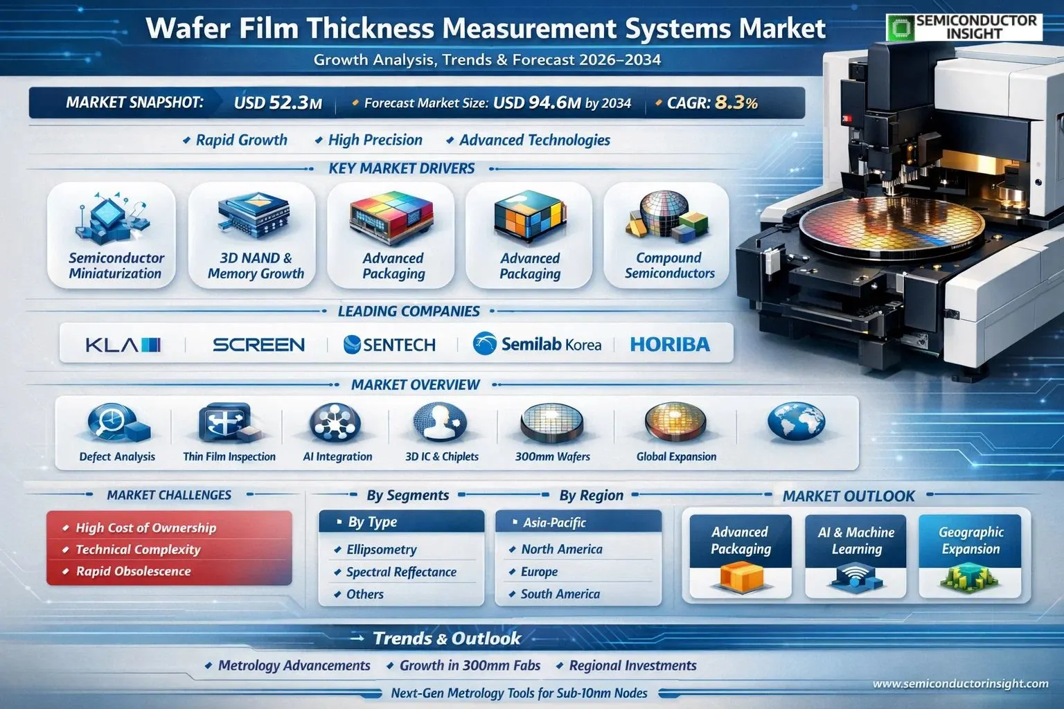
MARKET DRIVERS
Surge in Semiconductor Miniaturization and Advanced Node Development
The relentless drive toward smaller, more powerful chips is a primary enabler for the Wafer Film Thickness Measurement Systems Market. As semiconductor manufacturers transition to sub-7nm and 3nm process nodes, the precision required for films like high-k gate dielectrics, epitaxial silicon, and ultra-thin barriers measured in angstroms is paramount. This demand for extreme metrology accuracy directly fuels investments in advanced optical, ellipsometry, and X-ray based measurement systems essential for process control and yield management.
Expansion of 3D NAND and Advanced Memory Fabrication
The proliferation of 3D NAND flash memory, characterized by its vertical stack of memory cells, has created a critical need for precise layer-by-layer thickness monitoring. The Wafer Film Thickness Measurement Systems Market is propelled by this architecture, where uniformity across dozens of stacked films directly impacts device performance and storage density. Similar demands arise from the manufacturing of cutting-edge DRAM and emerging memories like MRAM.
➤ The need for non-destructive, high-throughput metrology is non-negotiable in modern fabs, making in-line and integrated measurement systems a cornerstone of production.
Furthermore, the rise of compound semiconductors (GaN, SiC) for power electronics and 5G RF devices introduces new material sets that require specialized metrology solutions, broadening the application scope and technological requirements within the Wafer Film Thickness Measurement Systems Market.
MARKET CHALLENGES
Technical Complexity and Integration Hurdles at Leading-Edge Nodes
As feature sizes shrink, traditional optical metrology faces significant challenges due to proximity effects and pattern-induced inaccuracies. Characterizing films within high-aspect-ratio structures or complex 3D features often requires the integration of multiple measurement techniques, increasing system complexity and cost. Ensuring measurement precision on new material stacks, such as novel metal gates and low-k dielectrics, presents ongoing R&D challenges for equipment vendors.
Other Challenges
High Cost of Ownership and Operational Expertise
Advanced Wafer Film Thickness Measurement Systems represent a significant capital investment. Beyond acquisition, the total cost of ownership includes calibration, maintenance, and the need for highly skilled personnel to operate the systems and interpret complex data, which can be a barrier for smaller foundries and research facilities.
Rapid Technological Obsolescence
The fast pace of semiconductor process evolution can render specific metrology tools obsolete quickly. Manufacturers in the Wafer Film Thickness Measurement Systems Market must continuously innovate, risking that new process integration requirements may outpace the development cycle of their latest systems.
MARKET RESTRAINTS
Capital Expenditure Cyclicality in the Semiconductor Industry
The Wafer Film Thickness Measurement Systems Market is inherently tied to the capital investment cycles of major semiconductor manufacturers. During periods of oversupply or economic downturn, chipmakers often delay or reduce equipment purchases, including metrology tools. This cyclicality creates revenue volatility for suppliers, as demand directly correlates with global fab construction and technology upgrade programs, which are subject to macroeconomic pressures.
Intense Competitive Pressure and Price Sensitivity
The market features a concentrated group of established global players competing intensely on technology, service, and price. This competition can pressure profit margins and lead to price-sensitive purchasing decisions by large foundries and IDMs, who often negotiate large-volume deals. This environment can restrain the growth potential for smaller or newer entrants in the Wafer Film Thickness Measurement Systems Market.
MARKET OPPORTUNITIES
Growth in Heterogeneous Integration and Advanced Packaging
The industry shift toward heterogeneous integration, chiplets, and 2.5D/3D advanced packaging opens a significant growth avenue. These architectures require precise thickness measurement of interposers, redistribution layers, micro-bumps, and underfill materials. Metrology systems adaptable to these new packaging paradigms, beyond traditional front-end wafer processing, represent a key expansion opportunity for the Wafer Film Thickness Measurement Systems Market.
Adoption of AI and Machine Learning for Predictive Metrology
The integration of artificial intelligence and machine learning algorithms with measurement systems creates opportunities for predictive process control and enhanced yield analysis. AI can optimize measurement recipes, identify drift in tool performance, and correlate film thickness data with final device electrical parameters. This shift from simple measurement to predictive analytics and insight generation adds substantial value, creating a premium market segment.
Geographic Expansion of Semiconductor Manufacturin
Government initiatives and supply chain diversification efforts are driving massive new fab investments in regions like the United States, Europe, Japan, and Southeast Asia. Each new state-of-the-art fabrication facility requires a full suite of process control equipment, generating sustained demand for Wafer Film Thickness Measurement Systems. This geographic expansion lessens regional demand concentration and provides a stable, long-term growth driver for the market.
Significant Wafer Film Thickness Measurement Systems Market Trends
Technological Advancement in Metrology Tools
The evolution of measurement technologies like ellipsometry and spectral reflectance is a dominant trend in the Wafer Film Thickness Measurement Systems Market. As semiconductor nodes shrink to 3nm and below, the demand for non-contact, high-precision systems with angstrom-level resolution and faster throughput intensifies. Manufacturers are integrating advanced algorithms and machine learning to enhance data analysis, improve uniformity mapping, and predict process deviations in real-time. This progression is critical for controlling complex multi-layer film stacks in advanced logic and memory devices, ensuring stringent quality standards are met. This technical progression in metrology for semiconductor manufacturing is a primary demand driver.
Other Trends
Growing Application in 300mm Wafer Fabs
The expansion of 300mm wafer fabrication capacity globally is a significant trend shaping the Wafer Film Thickness Measurement Systems Market. New fabs and capacity expansions, particularly for advanced nodes, require a substantial number of new measurement tools. This segment represents the largest and most critical application area, as 300mm wafers are the standard for leading-edge semiconductor production. The need for in-line monitoring and statistical process control within these high-volume manufacturing environments directly fuels sales and development efforts for system vendors. Adoption rates in 200mm fabs for mature nodes and specialty semiconductors also remain steady, supporting a diverse market base.
Intensified Regional Competition and Supply Chain Focus
Geopolitical factors and supply chain security concerns are prompting regional investment trends that impact the Wafer Film Thickness Measurement Systems Market. Major initiatives in North America, Europe, and Asia-Pacific to establish resilient, domestic semiconductor manufacturing ecosystems are creating new demand pockets. This environment intensifies competition among established global manufacturers like KLA Instruments, Onto Innovation, and HORIBA, alongside regional players. The trend encourages localized service, support, and collaborative development to meet specific regional fab requirements and technical challenges, influencing strategic partnerships and market dynamics.
COMPETITIVE LANDSCAPE
Key Industry Players
A Market Defined by Precision, Innovation, and Intense Rivalry
Global wafer film thickness measurement systems market, projected to grow significantly by 2034, is dominated by a concentrated group of established metrology specialists. KLA Corporation, through its Instruments division, is widely recognized as the market leader, setting the benchmark for precision and integrated process control in high-volume semiconductor manufacturing. Its dominance is reinforced by a comprehensive portfolio catering to advanced nodes. Close behind, SCREEN Semiconductor Solutions and Onto Innovation hold substantial market shares, providing critical solutions across the fabrication process, from deposition to chemical mechanical planarization. The competitive structure is characterized by high technological barriers, where continuous R&D in techniques like spectroscopic ellipsometry and reflectometry is essential to maintain relevance. Market dynamics are further shaped by strategic mergers, acquisitions, and deep partnerships with leading semiconductor foundries and IDMs.
Beyond the top-tier players, a range of proficient companies occupy vital niches. Bruker and HORIBA leverage their expertise in analytical instrumentation to offer highly accurate spectroscopic tools. Specialized firms like SENTECH and n&k Technology provide focused solutions for research and development as well as specific production applications. Companies such as Film Sense and Semilab Korea are notable for their innovative optical measurement technologies. Furthermore, giants like Park Systems are expanding from their core atomic force microscopy base into the thin-film metrology space. The competitive intensity drives constant innovation in speed, non-destructiveness, and measurement capabilities for increasingly complex multi-layer stacks and new materials.
List of Key Wafer Film Thickness Measurement Systems Companies Profiled
- KLA Instruments
- SCREEN Semiconductor Solutions
- SENTECH
- Semilab Korea
- HORIBA
- Bruker
- n&k Technology
- Onto Innovation
- Film Sense
- Park Systems
- Nanometrics (now part of Onto Innovation)
- Rudolph Technologies (now part of Onto Innovation)
- Angstrom Sun Technologies Inc.
Segment Analysis:
| Segment Category | Sub-Segments | Key Insights |
| By Type |
|
Ellipsometry is the cornerstone technology, prized for its unparalleled precision and comprehensive material characterization capabilities beyond mere thickness. Its adoption is driven by the escalating complexity of semiconductor device architectures requiring multi-layer film analysis. The system’s ability to provide detailed insights into optical constants and film uniformity makes it indispensable for advanced research and development nodes, ensuring rigorous process control for high-value semiconductor production. |
| By Application |
|
300mm Wafer applications dominate demand, fueled by their central role in high-volume manufacturing of leading-edge logic and memory chips. The larger wafer size offers superior economies of scale but demands measurement systems with superior throughput, automation, and whole-wafer mapping capabilities to maintain yield. This segment’s growth is intrinsically linked to investments in new fabrication facilities for cutting-edge semiconductor technologies, where precision metrology is non-negotiable for profitability and performance. |
| By End User |
|
Foundries represent the most critical and demanding end-user segment, acting as the primary growth engine for the market. Their pure-play manufacturing model necessitates the highest standards of process control and yield management across diverse client designs, driving continuous investment in the latest metrology solutions. The intense competition among major foundries to offer superior process technology and wafer yields creates a persistent, high-value demand for advanced film thickness measurement systems that enhance operational efficiency and customer trust. |
| By Technology Node |
|
Advanced Nodes are the primary value driver, demanding the most sophisticated and precise measurement solutions. As feature sizes shrink to atomic scales, film thickness control becomes exponentially more critical, with tolerances measured in angstroms. This necessitates measurement systems with exceptional resolution, stability, and advanced algorithms to account for material and structural complexities. The relentless industry push for miniaturization and performance ensures sustained R&D focus and premium pricing for systems capable of supporting these frontier manufacturing processes. |
| By Integration |
|
Integrated Metrology (In-line) is increasingly viewed as the strategic direction for high-volume manufacturing, owing to its compelling advantages in fab productivity. By embedding measurement directly into process tools, it enables real-time, closed-loop process control, drastically reducing measurement lag time and wafer handling. This integration is crucial for advanced process control strategies, minimizing scrap and accelerating yield ramps. The trend towards Smart Manufacturing and Industry 4.0 in semiconductor fabs is a significant tailwind, prioritizing seamless data flow and automated process correction that in-line systems uniquely provide. |
Regional Analysis: Wafer Film Thickness Measurement Systems Market
Asia-Pacific
This cluster is the epicenter of the most advanced Wafer Film Thickness Measurement Systems demand. Taiwan’s TSMC and South Korea’s Samsung and SK Hynix operate at the bleeding edge of process technology, requiring metrology for complex multi-patterning, new materials like High-K Metal Gates, and 3D NAND stacks. The relentless pace of node transitions here sets Global benchmark for system capabilities.
China’s market is characterized by massive government-backed investment aimed at achieving semiconductor independence. This drives demand across the spectrum, from mature-node measurement systems for power and analog chips to advanced tools for logic and memory. The focus is on rapidly scaling domestic production capacity, creating a vast and diverse market for measurement solutions.
Japan retains a leading role through its dominance in critical semiconductor materials and precision equipment. Japanese fabs and R&D centers demand high-precision wafer film thickness measurement systems for developing next-generation materials and processes. The ecosystem’s strength in compound semiconductors and sensors also fuels specialized metrology needs.
This sub-region is growing in importance for the Wafer Film Thickness Measurement Systems Market, particularly for systems tailored to advanced packaging. As assembly, testing, and packaging operations expand in Malaysia, Vietnam, and India, the demand for metrology to control film thickness in fan-out wafer-level packaging and 3D integration schemes is increasing significantly.
North America
North America, primarily the United States, holds a strategically vital position in the Wafer Film Thickness Measurement Systems Market as the center for R&D, design, and the headquarters of major integrated device manufacturers (IDMs) like Intel. While its volume of wafer fabrication is less than Asia-Pacific, its influence on technology roadmaps is immense. The market demand is driven by leading-edge logic development, cutting-edge research in national labs and universities, and the production of high-value, low-volume chips for aerospace, defense, and specialized computing. This results in a need for highly sophisticated, often customized measurement systems capable of characterizing novel materials and architectures very early in the development cycle. The close collaboration between metrology suppliers, chip designers, and process development teams in this region fosters a strong innovation feedback loop.
Europe
The European market for Wafer Film Thickness Measurement Systems is characterized by specialization and high-value manufacturing. Key demand stems from automotive semiconductor fabs, particularly in Germany, which require robust and reliable metrology for power devices, sensors, and microcontrollers built on mature and specialized nodes. Furthermore, Europe is a leader in research infrastructure, with institutes like IMEC driving advancements that require precise measurement for new semiconductor materials and photonics. The market also sees steady demand from the industrial and medical semiconductor segments, where precision and quality control over film thickness are paramount. European manufacturers often prioritize measurement solutions that offer high stability, traceability, and integration with advanced process control systems.
South America
The South American market for Wafer Film Thickness Measurement Systems is nascent but developing, primarily focused on supporting regional electronics assembly and certain niche industrial applications. Currently, demand is largely for refurbished or entry-level systems used in academic research, small-scale prototyping, and quality control for basic semiconductor components used in consumer electronics assembly. Brazil is the most active country, with some local manufacturing of simpler integrated circuits and sensors. The market potential is tied to broader regional economic development and any future government initiatives to build strategic technology sectors. For now, it represents a secondary market for established global suppliers of wafer film thickness measurement systems.
Middle East & Africa
The Wafer Film Thickness Measurement Systems Market in the Middle East & Africa region is in its early stages, with demand concentrated almost exclusively in a few technology hubs. Initiatives like Saudi Arabia’s NEOM and various smart city projects are driving initial investments in local semiconductor R&D and design, which may create future demand for metrology tools for prototyping. The United Arab Emirates also shows interest in building a tech ecosystem. Currently, any systems present are primarily for academic research or supporting minor electronics manufacturing. Africa’s market is negligible, with very limited local semiconductor activity. The region’s growth is contingent on long-term, large-scale investments materializing to create a foundational semiconductor manufacturing base.
Report Scope
This market research report provides a comprehensive analysis of the Wafer Film Thickness Measurement Systems Market, covering the forecast period 2026–2034. It offers detailed insights into market dynamics, technological advancements, competitive landscape, and key trends shaping the industry.
Key focus areas of the report include:
- Market Overview: The report begins with an overview outlining its current market scenario, key growth indicators, and industry transformation drivers. It discusses macroeconomic factors, demand–supply balance, regulatory landscape, and the strategic role of semiconductors in powering advancements across industries such as automotive, telecommunications, consumer electronics, and industrial automation.
- Market Size & Forecast: Historical data and future projections for revenue, unit shipments, and market value across major regions and segments.
- Segmentation Analysis: Detailed breakdown by product type, technology, application, and end-user industry to identify high-growth segments and investment opportunities.
- Regional Insights: Insights into market performance across North America, Europe, Asia-Pacific, Latin America, and the Middle East & Africa, including country-level analysis where relevant.
- Competitive Landscape: Profiles of leading market participants, including their product offerings, R&D focus, manufacturing capacity, pricing strategies, and recent developments such as mergers, acquisitions, and partnerships.
- Technology Trends & Innovation: Assessment of emerging technologies, integration of AI/IoT, semiconductor design trends, fabrication techniques, and evolving industry standards.
- Market Drivers & Restraints: Evaluation of factors driving market growth along with challenges, supply chain constraints, regulatory issues, and market-entry barriers.
- Stakeholder Insights: Insights for component suppliers, OEMs, system integrators, investors, and policymakers regarding the evolving ecosystem and strategic opportunities.
Primary and secondary research methods are employed, including interviews with industry experts, data from verified sources, and real-time market intelligence to ensure the accuracy and reliability of the insights presented.
FREQUENTLY ASKED QUESTIONS:
What is the current market size and growth forecast for the Wafer Film Thickness Measurement Systems Market?
-> Global Wafer Film Thickness Measurement Systems Market was valued at USD 52.3 million in 2025 and is projected to reach USD 94.6 million by 2034, growing at a CAGR of 8.3% during the forecast period.
Which key companies operate in the Wafer Film Thickness Measurement Systems Market?
-> Key players include KLA Instruments, SCREEN Semiconductor Solutions, SENTECH, Semilab Korea, HORIBA, Bruker, n&k Technology, Onto Innovation, Film Sense, and Park Systems, among others. In 2025, Global top five players held a significant revenue share.
What are the primary applications of Wafer Film Thickness Measurement Systems?
->Systems are critical for measuring and analyzing thin film properties on semiconductor wafers to ensure quality for high-precision electronic devices. Key applications include 300mm wafers, 200mm wafers, and other wafer sizes.
What are the main technology segments in this market?
-> The market is segmented by technology type, which includes Ellipsometry, Spectral Reflectance, and Others. The Ellipsometry segment is a significant contributor to market growth.
Which regions are covered in the market analysis?
-> The report provides detailed regional analysis covering North America, Europe, Asia, South America, and the Middle East & Africa, with country-level breakdowns for major markets including the U.S., China, Japan, South Korea, and Germany.

Get Sample Report PDF for Exclusive Insights
Report Sample Includes
- Table of Contents
- List of Tables & Figures
- Charts, Research Methodology, and more...
 Download Sample Report PDF


