Wafer Dicing Blade Market Insights
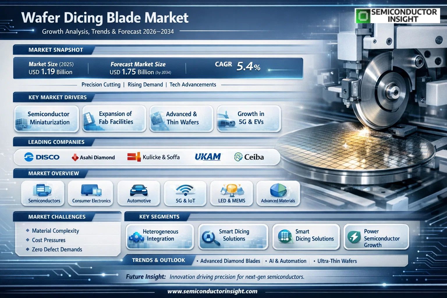
Global wafer dicing blade market size was valued at USD 1.19 billion in 2025. The market is projected to grow from USD 1.25 billion in 2026 to USD 1.75 billion by 2034, exhibiting a CAGR of 5.4% during the forecast period.
A wafer dicing blade is a high-precision cutting tool primarily used in the semiconductor industry to slice wafers into individual chips or dies. This blade is designed to make precise, clean cuts in silicon wafers, ceramics, glass, and other materials commonly used in electronics and semiconductor manufacturing. The process of wafer dicing is a critical step in the production of semiconductor devices, such as integrated circuits (ICs), LEDs, and MEMS (Microelectromechanical systems), where the wafer must be divided into individual, functional components.
The market is experiencing steady growth due to several factors, including the relentless demand for smaller and more powerful semiconductor devices across consumer electronics, automotive, and telecommunications sectors. Furthermore, advancements in blade technology,such as improved diamond abrasives and advanced bonding methods,are enhancing cutting precision and tool longevity. Initiatives by key players are also expected to fuel market growth. For instance, leading companies like DISCO Corporation and Tokyo Seimitsu continuously invest in R&D to develop thinner blades capable of handling next-generation materials like silicon carbide (SiC) and gallium nitride (GaN). DISCO Corporation, Asahi Diamond Industrial Co., Ltd., Kulicke & Soffa Industries Inc., UKAM Industrial Superhard Tools Inc., and Ceiba Technologies are some of the key players that operate in the market with a wide range of portfolios.
MARKET DRIVERS
Expansion of Semiconductor Fabrication Facilities
Global surge in demand for semiconductors, particularly for advanced computing, automotive electronics, and 5G infrastructure, is driving significant capital expenditure in new fabrication plants. This expansion directly fuels demand for consumables like the wafer dicing blade, as each new production line requires a consistent, high-volume supply of these precision tools for singulating individual die.
Adoption of Advanced and Ultra-Thin Wafers
The trend towards miniaturization and higher-density packaging, such as fan-out wafer-level packaging (FOWLP) and 3D IC integration, necessitates the processing of thinner and more fragile wafers. This places a premium on dicing blades engineered for minimal chipping, superior cut quality, and reduced mechanical stress, thereby propelling innovation and adoption of next-generation blade technologies in the wafer dicing blade market.
➤ The relentless push for higher productivity in semiconductor manufacturing is a critical factor for the wafer dicing blade market, with blade longevity and cut speed being key purchase drivers.
Additionally, the proliferation of compound semiconductors like silicon carbide (SiC) and gallium nitride (GaN) for power electronics and RF applications creates specialized demand. Dicing these harder, more brittle materials requires blades with diamond grit formulations and bond systems distinct from those used for traditional silicon, opening a high-value segment within the overall market.
MARKET CHALLENGES
Technical Complexity in Dicing Advanced Materials
A primary challenge for suppliers in the wafer dicing blade market is keeping pace with the evolving material science of semiconductors. Dicing new substrate materials and complex multilayered structures without inducing micro-cracks or delamination requires continuous R&D investment. Each new material or device architecture often demands a customized blade solution, increasing development costs and time-to-market.
Other Challenges
Price Sensitivity and Operational Cost Pressure
While blade performance is critical, semiconductor manufacturers operate under intense cost pressures. This creates a challenging environment for wafer dicing blade vendors, who must balance the higher costs of advanced abrasives and manufacturing with the customer’s need to control the cost-per-consumable. This often limits pricing power for premium products.
Requirement for Zero Defect Manufacturing
The industry’s shift towards zero-defect paradigms in high-reliability sectors like automotive places extreme scrutiny on the consistency and fault prediction of consumables. Any variability in a wafer dicing blade’s performance can lead to catastrophic yield loss, forcing blade manufacturers to implement rigorous quality control and lot-traceability systems that add significant overhead.
MARKET RESTRAINTS
Cyclical Downturns in the Semiconductor Industry
The wafer dicing blade market is inherently tied to the capital investment cycles of the broader semiconductor industry. During periods of inventory correction or reduced end-demand, chipmakers delay or cancel expansion plans and extend the life of existing consumables. This cyclicality can lead to volatile order patterns and revenue streams for blade manufacturers, constraining steady market growth.
Furthermore, the emergence and incremental adoption of alternative die-separation technologies, such as stealth dicing (laser-based) and plasma dicing, present a technological restraint. Although these methods are not suitable for all materials and are often used in hybrid processes with blade dicing, they capture specific high-value applications, potentially capping the growth rate of the traditional mechanical wafer dicing blade market in certain segments.
MARKET OPPORTUNITIES
Growth in Heterogeneous Integration and Chiplet Architectures
The industry’s move towards heterogeneous integration, where multiple dissimilar chips or chiplets are packaged together, creates a robust opportunity. This trend often involves dicing reconstituted wafers or panels containing diverse die, which can be more challenging than standard silicon. Tailored wafer dicing blade solutions for these complex substrates represent a significant value-added market segment.
Integration of Industry 4.0 and Predictive Analytics
There is a substantial opportunity to evolve the wafer dicing blade from a passive consumable to a smart component. By integrating sensors or leveraging machine learning on dicing tool data, blade wear and potential failure can be predicted. This enables predictive maintenance, optimizes blade change schedules, and minimizes unscheduled downtime, offering a compelling value proposition that can command a premium in the wafer dicing blade market.
The sustained global focus on electrification of vehicles and renewable energy infrastructure guarantees long-term demand for power semiconductors. This directly benefits the wafer dicing blade market, as manufacturing SiC and GaN devices at scale will require a massive, reliable supply of specialized dicing blades capable of handling these tough materials efficiently and with high yield.
Wafer Dicing Blade Market Trends
Technological Refinement for Advanced Nodes
A primary trend in the Wafer Dicing Blade Market is the continuous evolution of blade technology to meet the demands of advanced semiconductor nodes. As chip features shrink below 7nm and 5nm, the mechanical and thermal stress induced during dicing becomes a critical yield factor. This has led to innovation in advanced high-grade diamonds and precisely engineered bonding matrices. These materials are designed to create blades that deliver ultra-fine, clean cuts with minimal chipping and subsurface damage. The trend is tightly linked to the growing need for high-quality dicing of complex materials like ultra-low-k dielectrics and compound semiconductors used in 5G and high-performance computing devices.
Other Trends
Material and Bonding Diversification
The selection of a suitable wafer dicing blade is increasingly application-specific, driving diversification in materials and bonds. Resin-bonded blades, known for providing excellent surface finish and low force cutting, are favored for delicate and brittle materials. Metal-bonded blades offer superior durability and higher cutting speeds for tougher substrates. Recent developments in hybrid bonding methods are creating blades that balance cutting speed with edge quality, optimizing performance for high-mix manufacturing environments. This trend supports the production of a wider array of devices, from large power modules to miniature IoT sensors.
Integration with Smart Dicing Systems
A significant industrial trend is the integration of wafer dicing blades with intelligent, automated dicing systems. Modern saws are equipped with in-process monitoring and adaptive control technologies that adjust feed rates and spindle speeds in real-time based on blade wear and material properties. This places new demands on blade consistency and predictability. Manufacturers are responding by providing blades with highly uniform abrasive distribution and tighter dimensional tolerances to ensure seamless integration with these systems. The overall trend moves the Wafer Dicing Blade Market toward a data-driven ecosystem where blade performance is a key input for maximizing yield and optimizing the total cost of ownership in semiconductor production.
COMPETITIVE LANDSCAPE
Key Industry Players
Analysis of Global Wafer Dicing Blade Segment
Global wafer dicing blade market is characterized by a moderate concentration where technological expertise and material science innovation are primary competitive differentiators. DISCO Corporation stands as the undisputed market leader, commanding significant share due to its comprehensive product portfolio, deep integration with precision dicing saws, and a reputation for exceptional blade longevity and cutting precision. The competitive structure is bifurcated, with a handful of large, diversified industrial corporations like Asahi Diamond Industrial, 3M, and Saint-Gobain leveraging their advanced materials and abrasives capabilities. These players dominate through extensive R&D investments and global supply chains, catering to high-volume semiconductor foundries. Alongside them, specialized manufacturers such as Kulicke & Soffa Industries and Tokyo Seimitsu compete by offering optimized blade solutions tailored to their proprietary semiconductor assembly and test equipment.
Beyond the top-tier vendors, a robust ecosystem of niche and regional players addresses specific application needs and cost-sensitive markets. Companies like Kinik, Ceiba, and UKAM are significant for their expertise in specific bonding technologies and grit formulations for materials like ceramics and advanced compound semiconductors used in LEDs and power devices. The Asia-Pacific region, particularly Japan, China, and Taiwan, is a hotbed for both consumption and manufacturing, with firms like Shanghai Sinyang, Xiamen Tungsten, and Nanjing Sanchao Advanced Materials strengthening the regional supply base. These players often compete on agility, customization, and price, serving emerging fabless companies and contract manufacturers. The market sees continuous pressure for innovation in diamond grain integrity and bonding agents to meet the demands of ultra-thin wafers and heterogeneous integration, keeping competition intense across all tiers.
List of Key Wafer Dicing Blade Companies Profiled
- DISCO Corporation
- Asahi Diamond Industrial Co., Ltd.
- Kulicke & Soffa Industries, Inc.
- UKAM Industrial Superhard Tools
- Ceiba Technologies
- Shanghai Sinyang Semiconductor Materials Co., Ltd.
- ITI (International Technical Industries)
- Kinik Company
- Saint-Gobain S.A.
- Tokyo Seimitsu Co., Ltd.
- 3M Company
- Lam Research Corporation
- Xiamen Tungsten Co., Ltd.
- Sungold Abrasives Co., Ltd.
Segment Analysis:
| Segment Category | Sub-Segments | Key Insights |
| By Type |
|
Hub Dicing Blades are a leading category due to their structural stability and widespread adoption in conventional dicing saws. These blades offer significant mechanical rigidity, which is critical for maintaining precise kerf control and reducing blade deflection during high-speed cutting operations. Their design facilitates easier mounting and dismounting, streamlining integration into automated production lines and reducing tool changeover downtime. This segment’s dominance is further reinforced by its ability to handle a broad spectrum of wafer materials, from silicon to advanced compound semiconductors, making it a versatile and reliable choice for established manufacturing workflows in high-volume fabs. |
| By Application |
|
Integrated Circuits (IC) represent the primary and most demanding application segment, driven by the unrelenting global demand for computing power and data processing. This segment necessitates blades capable of executing ultra-fine, clean cuts on increasingly thin and complex silicon wafers to maximize the number of functional dies per wafer. The push toward advanced logic and memory nodes below 10nm requires dicing technologies that minimize micro-cracking and chipping to preserve wafer integrity. Furthermore, the growth of specialty ICs for automotive, AI, and 5G applications is creating a sustained need for high-precision dicing solutions that can support heterogeneous integration and complex multi-chip packaging architectures. |
| By End User |
|
Semiconductor Device Manufacturers (IDMs) are a dominant end-user segment, as they require tightly controlled, integrated manufacturing processes for premium components. Their in-house dicing operations demand blades that deliver exceptional yield, consistency, and tool life to meet stringent internal quality benchmarks and production schedules. This segment’s leadership is underpinned by substantial investment in next-generation dicing equipment and proprietary blade specifications tailored for cutting-edge device architectures. The critical need to protect intellectual property linked to novel materials and device structures also incentivizes these manufacturers to work closely with blade suppliers on custom developments, securing a pipeline for advanced, application-specific blade solutions. |
| By Material Bonding |
|
Resin Bond blades are the leading material bonding segment, favored for their superior ability to provide smoother cut surfaces with reduced mechanical stress on delicate wafers. This bonding technology excels in applications requiring high surface finish quality and minimal subsurface damage, which is essential for maintaining the electrical performance of sensitive components. The inherent elasticity of the resin matrix allows for better shock absorption during cutting, thereby lowering the incidence of micro-fractures that can compromise device reliability. This segment’s growth is further propelled by ongoing advancements in resin formulations that enhance heat dissipation and extend blade lifespan, aligning with the industry’s need for cost-effective, high-performance consumables in volume production. |
| By Precision Requirement |
|
High-Precision/Ultra-Fine Dicing is the leading and fastest-evolving segment, directly fueled by the industry-wide trend toward device miniaturization and functional density enhancement. This segment demands blades with extremely fine grits and advanced geometric tolerances to achieve sub-micron accuracy in kerf width and exceptional positional repeatability. The critical drivers for this segment include the fabrication of micro-electromechanical systems (MEMS), advanced sensor arrays, and power devices where clean, narrow streets are vital for maximizing die count and performance. Innovations here are concentrated on developing blades that combine minimal cutting force with high thermal stability to protect delicate nanostructures, making this the focal point for technological differentiation and value creation among leading suppliers. |
Regional Analysis: Wafer Dicing Blade Market
Asia-Pacific
The concentration of leading-edge foundries and memory chip manufacturers creates a captive market for ultra-precision dicing blades, with a focus on minimizing chipping and maximizing die yield for next-generation nodes, especially in Taiwan and South Korea.
Local blade manufacturers in Japan and South Korea are at the forefront of developing dicing blades for new substrate materials, including Silicon Carbide (SiC) and glass wafers for MEMS and photonics applications.
Proximity to major tool integrators and wafer fabs allows for rapid prototyping and customization of dicing blades, reducing lead times and enabling collaborative development of blade specifications.
A mature ecosystem for abrasive materials and tooling components, particularly in China and Southeast Asia, enables the production of both high-volume commodity dicing blades and specialized premium products.
North America
North America’s Wafer Dicing Blade market is characterized by high-value, innovation-driven demand centered on research, development, and niche manufacturing. The region, led by the United States, is a hotbed for fabless semiconductor companies and integrated device manufacturers (IDMs) that design cutting-edge chips, which are then often assembled and packaged using advanced dicing processes, even if outsourced. This drives a need for specialized, high-performance dicing blades for prototypes, low-volume/high-mix production, and novel materials like those used in quantum computing and defense applications. The market is heavily influenced by investments from key players in the automotive (for power electronics) and telecommunications (for RF filters) sectors, where precision and blade longevity for compound semiconductors are critical. Strategic partnerships between blade suppliers and equipment OEMs are a defining feature of the regional dynamic.
Europe
The European market for Wafer Dicing Blades is a sophisticated segment focused on quality, precision engineering, and specialized industrial applications. Germany, the Netherlands, and France are key contributors, with demand stemming from the automotive industry’s shift to electrification (requiring SiC dicing), the strong industrial sensor and power module sector, and the presence of major semiconductor equipment manufacturers. The regional focus is less on commodity, high-volume production and more on developing and procuring blades that offer superior process stability, low Total Cost of Ownership (TCO), and compatibility with highly automated dicing saw lines used in advanced packaging techniques like fan-out wafer-level packaging (FOWLP). Environmental regulations also subtly influence blade development towards longer lifecycles and reduced consumable waste.
South America
The South American market for Wafer Dicing Blade currently represents a smaller, emerging segment largely tied to electronics manufacturing services (EMS) and assembly operations, primarily in Brazil. The demand is driven by the packaging and testing of imported semiconductor components for consumer electronics and the automotive aftermarket. The market is characterized by a focus on cost-effective, reliable standard dicing blades for mainstream silicon wafer applications rather than cutting-edge solutions. Growth is linked to regional government incentives to attract electronics manufacturing, but it remains constrained by the lack of a significant local semiconductor fabrication base. Blade suppliers typically service this region through distribution partnerships.
Middle East & Africa
Demand in the Middle East & Africa for Wafer Dicing Blade is nascent but shows potential for niche growth in specific sectors. Investment in technological diversification, particularly in Gulf Cooperation Council (GCC) nations, could spur demand for blades used in downstream electronics assembly for consumer goods. The primary regional demand currently stems from limited university and research institute activities in materials science and microelectronics, requiring small quantities of precision blades for R&D on new semiconductor materials. The market is served almost exclusively by global distributors, with no significant local manufacturing presence. Long-term prospects are tied to large-scale technology hub initiatives and their success in attracting downstream electronics manufacturing.
Report Scope
This market research report provides a comprehensive analysis of the Wafer Dicing Blade Market , covering the forecast period 2026–2034. It offers detailed insights into market dynamics, technological advancements, competitive landscape, and key trends shaping the industry.
Key focus areas of the report include:
- Market Overview: The report begins with an overview outlining its current market scenario, key growth indicators, and industry transformation drivers. It discusses macroeconomic factors, demand–supply balance, regulatory landscape, and the strategic role of semiconductors in powering advancements across industries such as automotive, telecommunications, consumer electronics, and industrial automation.
- Market Size & Forecast: Historical data and future projections for revenue, unit shipments, and market value across major regions and segments.
- Segmentation Analysis: Detailed breakdown by product type, technology, application, and end-user industry to identify high-growth segments and investment opportunities.
- Regional Insights: Insights into market performance across North America, Europe, Asia-Pacific, Latin America, and the Middle East & Africa, including country-level analysis where relevant.
- Competitive Landscape: Profiles of leading market participants, including their product offerings, R&D focus, manufacturing capacity, pricing strategies, and recent developments such as mergers, acquisitions, and partnerships.
- Technology Trends & Innovation: Assessment of emerging technologies, integration of AI/IoT, semiconductor design trends, fabrication techniques, and evolving industry standards.
- Market Drivers & Restraints: Evaluation of factors driving market growth along with challenges, supply chain constraints, regulatory issues, and market-entry barriers.
- Stakeholder Insights: Insights for component suppliers, OEMs, system integrators, investors, and policymakers regarding the evolving ecosystem and strategic opportunities.
Primary and secondary research methods are employed, including interviews with industry experts, data from verified sources, and real-time market intelligence to ensure the accuracy and reliability of the insights presented.
FREQUENTLY ASKED QUESTIONS:
What is the current market size of Wafer Dicing Blade Market?
-> Global Wafer Dicing Blade Market was valued at USD 1187 million in 2025 and is projected to reach USD 1754 million by 2034, growing at a CAGR of 5.4% during the forecast period.
Which key companies operate in Wafer Dicing Blade Market?
-> Key players include DISCO Corporation, Asahi Diamond Industrial, Kulicke & Soffa Industries, UKAM, Ceiba, Shanghai Sinyang, ITI, Kinik, Saint-Gobain, Tokyo Seimitsu, 3M, Lam Research Corporation, Xiamen Tungsten, Sungold Abrasives, Lande Precision Tools, Hongye Cutting Tools, Bosch Abrasives, Suzhou Sail Science & Technology Co., Ltd., Nanjing Sanchao Advanced Materials, System Technology, Thermocarbon, and YMB, among others.
What are the key growth drivers?
-> Key growth drivers include the growing demand for smaller, faster, and more powerful semiconductor devices, continued expansion of telecommunications, automotive, and consumer electronics industries, and trends like miniaturization, AI, IoT, and electric vehicles (EVs).
Which region dominates the market?
-> Asia is a key regional market, with significant demand and manufacturing presence in countries such as China, Japan, South Korea, and Southeast Asia.
What are the emerging trends?
-> Emerging trends include innovations in blade materials like advanced diamond coatings, improved bonding techniques, integration of AI-driven dicing equipment, and automation for faster and more precise cuts.

Get Sample Report PDF for Exclusive Insights
Report Sample Includes
- Table of Contents
- List of Tables & Figures
- Charts, Research Methodology, and more...
 Download Sample Report PDF