Wafer Acceptance Testing Market Insights
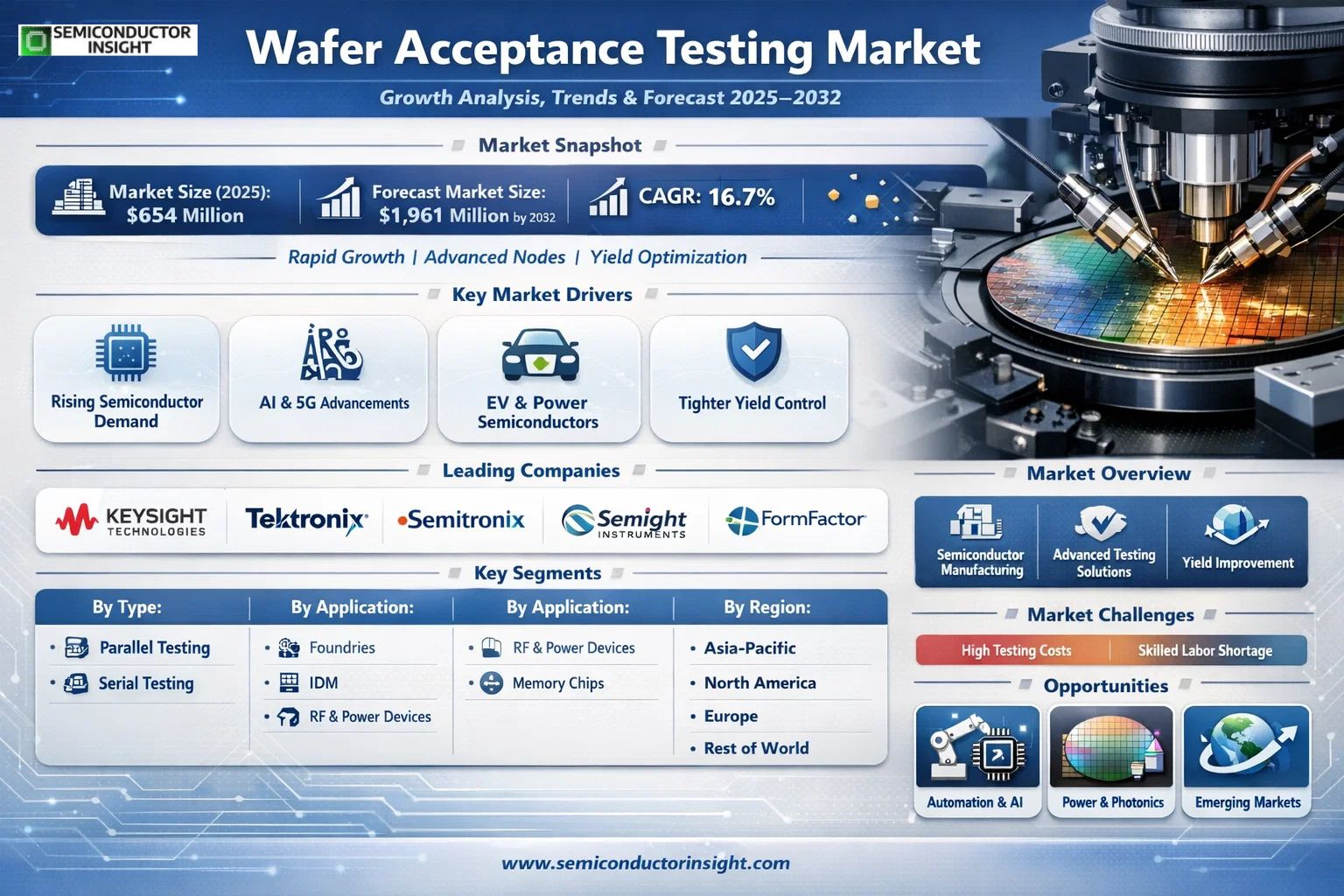
Global Wafer Acceptance Testing market size was valued at USD 654 million in 2025. The market is projected to reach USD 1,961 million by 2032, exhibiting a CAGR of 16.7% during the forecast period.
Wafer Acceptance Testing (WAT) is a critical wafer-level electrical characterization and process monitoring activity in semiconductor manufacturing, designed to evaluate whether wafer processes meet predefined electrical specifications and process stability requirements by measuring dedicated test structures such as resistors, capacitors, diodes, and transistors. Downstream customers mainly include foundries and IDM manufacturers across logic, memory, power semiconductor, and RF device segments, relying on WAT for early defect screening and yield optimization.
The market is experiencing robust growth driven by increasing process complexity, surging demand for advanced nodes, and tighter yield control in fabs. Furthermore, high technical barriers and strong customer stickiness support premium pricing, with global nominal production capacity at approximately 2,600 units in 2025, actual shipments around 1,080 units, and average selling price of about USD 663,000 per unit. Manufacturers typically achieve gross margins of 55%-65%. Key players including Keysight, Tektronix, Semitronix, and Semight lead with proven system integration and software capabilities.
MARKET DRIVERS
Surge in Semiconductor Demand
Wafer Acceptance Testing Market is propelled by the escalating global demand for semiconductors, particularly in consumer electronics, automotive, and data centers. As chip complexity increases with advanced nodes like 5nm and below, rigorous WAT ensures electrical parameters meet specifications, reducing downstream failures. Industry projections indicate semiconductor production growing at a CAGR of 8.5% through 2028, directly boosting WAT adoption.
Advancements in AI and 5G Technologies
Integration of AI chips and 5G infrastructure demands ultra-reliable wafers, where WAT verifies key metrics such as threshold voltage and leakage current. Major foundries report yield improvements of up to 15% post-WAT implementation, enhancing market confidence. This driver is evident in the rising wafer shipments, exceeding 16 million 300mm equivalents annually.
➤ Expansion into electric vehicles amplifies WAT necessity, with automotive semiconductors projected to reach $80 billion by 2027
Overall, these factors solidify Wafer Acceptance Testing Market’s growth trajectory amid digital transformation.
MARKET CHALLENGES
High Testing Costs and Complexity
Wafer Acceptance Testing Market faces hurdles from escalating costs associated with probing advanced nodes, where probe card wear and precision calibration drive expenses up by 20-30% per wafer. Smaller feature sizes complicate contact resistance, impacting test accuracy and throughput in high-volume manufacturing.
Other Challenges
Skilled Workforce Shortage
Aging expertise in WAT engineering limits scalability, as training for parametric testing on logic and memory wafers requires specialized knowledge, slowing market penetration in emerging fabs.
MARKET RESTRAINTS
Supply Chain Disruptions
Geopolitical tensions and raw material shortages, including silicon ingots, constrain Wafer Acceptance Testing Market by delaying wafer availability for testing. Foundry utilization rates hovering at 85-90% exacerbate bottlenecks, with lead times extending to 12-16 weeks.Regulatory compliance for cleanroom standards adds overhead, while equipment maintenance for WAT systems like DC testers demands significant CapEx, restraining smaller players.Volatility in chip pricing further pressures WAT investments, as cyclical downturns reduce testing volumes by up to 25% during inventory corrections.
MARKET OPPORTUNITIES
Automation and AI Integration
Wafer Acceptance Testing Market holds promise through automated probing and machine learning analytics, enabling predictive yield modeling and reducing manual interventions by 40%. This shift supports 24/7 operations in leading-edge fabs.Expansion into photonics and power semiconductors opens new avenues, with WAT adapting to SiC and GaN wafers for EV and renewable energy applications, tapping a $15 billion addressable segment by 2030.Emerging markets in Asia-Pacific drive outsourcing of WAT services, fostering partnerships that enhance global supply chain resilience and market accessibility.
Wafer Acceptance Testing Market Trends
Evolution Toward Higher Precision and Parallelism
In Wafer Acceptance Testing Market, a key trend is the shift toward equipment offering higher measurement precision, greater parallelism, and enhanced data processing capabilities. Advanced semiconductor process technologies require sensitive characterization of weak electrical signals from test structures like resistors, capacitors, diodes, and transistors. This drives innovation in measurement architectures, probing solutions, and noise suppression techniques, enabling better process monitoring and early defect screening in wafer fabrication.
Other Trends
Expansion in Parallel and Electrical Testing Segments
Parallel testing is gaining traction within Wafer Acceptance Testing Market due to its ability to handle higher throughput demands in volume production. Electrical testing remains dominant, focusing on wafer-level electrical characterization to ensure process stability. Combined with optical testing options, these segments support diverse applications across logic, memory, RF, and power wafers, where consistency and repeatability of results are critical for yield optimization.
Growth Driven by Foundry and IDM Applications
Foundries and integrated device manufacturers (IDMs) represent primary downstream customers in Wafer Acceptance Testing Market, integrating systems deeply into their yield management frameworks. Demand extends from process qualification to routine monitoring and cross-node benchmarking, with increasing emphasis on data reliability as fabs advance in automation and digitalization. This fosters long-term supplier partnerships due to high technical barriers and customer stickiness.
Emphasis on Software Differentiation and Data Integration
Software capabilities are emerging as a major differentiator in Wafer Acceptance Testing Market, transforming tools into platforms for analytics, modeling, and visualization. Integration with factory information systems enhances traceability across lots, supporting engineering decisions and process analysis. Leading players like Keysight and Tektronix leverage this to maintain market positions, amid challenges from specialized components and lengthy qualification cycles that shape competitive dynamics.
COMPETITIVE LANDSCAPE
Key Industry Players
Top Manufacturers in Wafer Acceptance Testing Equipment Market
Wafer Acceptance Testing (WAT) market exhibits a highly concentrated structure, dominated by established leaders such as Keysight Technologies and Tektronix, which command significant market share through their advanced parametric analyzers, probe stations, and integrated software solutions. These companies benefit from strong customer stickiness among leading foundries and IDMs, driven by deep integration with process nodes, yield management frameworks, and data environments. High technical barriers, including precision measurement capabilities and lengthy qualification cycles, reinforce their positions, with gross margins typically ranging from 55% to 65%. The market’s emphasis on reliability, repeatability, and traceability in electrical testing for logic, memory, RF, and power wafers further solidifies the dominance of these players in a segment projected to grow from USD 654 million in 2025 to USD 1,961 million by 2032 at a 16.7% CAGR.
Beyond the frontrunners, niche and significant players like Semitronix, Semight Instruments, and FormFactor provide specialized WAT systems, focusing on parallelism, noise suppression, and enhanced data analytics for routine production monitoring and cross-node benchmarking. Companies such as KLA Corporation and Advantest contribute probing and metrology expertise, while regional specialists including MPI Corporation and Tokyo Seimitsu (Accretech) cater to Asia-Pacific demand. Emerging challengers like Hprobe and Signatone target innovation in high-precision probing for advanced nodes, though competition remains shaped by technological depth, service capabilities, and long-term partnerships rather than frequent vendor switches. This landscape underscores the premium on software maturity and system integration amid rising automation in semiconductor fabs.
List of Key Wafer Acceptance Testing Companies Profiled
- Keysight Technologies
- Tektronix Inc.
- Semitronix Corporation
- Suzhou Semight Instruments Co., Ltd.
- FormFactor, Inc.
- KLA Corporation
- Advantest Corporation
- Teradyne, Inc.
- MPI Corporation
- Tokyo Seimitsu Co., Ltd. (Accretech)
- Hprobe
- Signatone Corporation
- MicroProbe, Inc.
Segment Analysis:
| Segment Category | Sub-Segments | Key Insights |
| By Type |
|
Parallel Testing
|
| By Application |
|
Foundry
|
| By End User |
|
Logic
|
| By Test Type |
|
Electrical Testing
|
| By Wafer Type |
|
Logic Wafers
|
Regional Analysis: Wafer Acceptance Testing Market
Explosive growth in electronics manufacturing propels Wafer Acceptance Testing Market, with fabs prioritizing inline testing to boost yields. High-volume production of memory and logic chips demands sophisticated protocols, while automotive sector mandates for reliability testing drive equipment upgrades.
Adoption of AI-driven defect detection and high-speed probing revolutionizes wafer acceptance in Asia-Pacific. Integration of machine learning for pattern recognition enhances accuracy, reducing false positives and enabling real-time process adjustments in Wafer Acceptance Testing Market.
Dense clusters of suppliers and service providers streamline Wafer Acceptance Testing Market operations. Proximity of testing facilities to fabs cuts logistics costs, fostering agility amid fluctuating demand and geopolitical shifts affecting semiconductor supply.
Stringent quality regulations and national semiconductor initiatives in Asia-Pacific bolster Wafer Acceptance Testing Market. Compliance with international standards like IATF 16949 ensures robust testing frameworks, supporting export competitiveness.
North America
North America plays a pivotal role in Wafer Acceptance Testing Market, driven by cutting-edge R&D from leading IDMs and fabs. Innovation hubs in the US focus on next-generation testing for advanced nodes, integrating photonics and quantum computing elements. The region’s Wafer Acceptance Testing Market benefits from strong IP ecosystems and venture funding, enabling early adoption of disruptive technologies like non-contact metrology. Automotive and data center applications demand ultra-reliable testing, prompting investments in automation. Collaborative efforts between academia and industry refine protocols, though higher costs challenge scalability. Overall, North America’s emphasis on quality and customization sustains its influence in the global Wafer Acceptance Testing Market landscape.
Europe
Europe’s Wafer Acceptance Testing Market is characterized by precision engineering and diversified applications. Key players in Germany and the Netherlands advance testing for power semiconductors and sensors, aligning with green energy transitions. Emphasis on sustainability drives eco-friendly testing solutions, reducing chemical usage in wafer processing. Wafer Acceptance Testing Market here integrates with automotive and industrial IoT sectors, where compliance with EU regulations ensures high standards. Research consortia foster cross-border innovations, enhancing yield analytics. Challenges include talent shortages, yet Europe’s mature infrastructure supports steady growth in specialized Wafer Acceptance Testing Market segments.
South America
South America emerges as a nascent player in Wafer Acceptance Testing Market, with Brazil leading assembly and testing services. Growing electronics localization efforts spur demand for basic wafer acceptance capabilities, supporting consumer goods and telecom. Infrastructure developments in fabs encourage technology transfers from Asia. Wafer Acceptance Testing Market faces hurdles like import dependencies and skill gaps, but cost advantages attract outsourcing. Regional collaborations aim to build expertise, positioning South America for gradual integration into global Wafer Acceptance Testing Market supply chains.
Middle East & Africa
The Middle East & Africa region witnesses budding activity in Wafer Acceptance Testing Market, anchored by UAE and Israel’s tech corridors. Focus on diversification beyond oil fuels semiconductor initiatives, emphasizing testing for defense and smart city projects. Partnerships with global firms introduce advanced Wafer Acceptance Testing Market tools, building local capacities. Africa’s nascent ecosystem targets mobile and renewable energy chips, grappling with energy reliability. Strategic investments promise expansion, enhancing the region’s foothold in the evolving Wafer Acceptance Testing Market.
Report Scope
This market research report provides a comprehensive analysis of the Wafer Acceptance Testing Market , covering the forecast period 2026–2034. It offers detailed insights into market dynamics, technological advancements, competitive landscape, and key trends shaping the industry.
Key focus areas of the report include:
- Market Overview: The report begins with an overview outlining its current market scenario, key growth indicators, and industry transformation drivers. It discusses macroeconomic factors, demand–supply balance, regulatory landscape, and the strategic role of semiconductors in powering advancements across industries such as automotive, telecommunications, consumer electronics, and industrial automation.
- Market Size & Forecast: Historical data and future projections for revenue, unit shipments, and market value across major regions and segments.
- Segmentation Analysis: Detailed breakdown by product type, technology, application, and end-user industry to identify high-growth segments and investment opportunities.
- Regional Insights: Insights into market performance across North America, Europe, Asia-Pacific, Latin America, and the Middle East & Africa, including country-level analysis where relevant.
- Competitive Landscape: Profiles of leading market participants, including their product offerings, R&D focus, manufacturing capacity, pricing strategies, and recent developments such as mergers, acquisitions, and partnerships.
- Technology Trends & Innovation: Assessment of emerging technologies, integration of AI/IoT, semiconductor design trends, fabrication techniques, and evolving industry standards.
- Market Drivers & Restraints: Evaluation of factors driving market growth along with challenges, supply chain constraints, regulatory issues, and market-entry barriers.
- Stakeholder Insights: Insights for component suppliers, OEMs, system integrators, investors, and policymakers regarding the evolving ecosystem and strategic opportunities.
Primary and secondary research methods are employed, including interviews with industry experts, data from verified sources, and real-time market intelligence to ensure the accuracy and reliability of the insights presented.
FREQUENTLY ASKED QUESTIONS:
What is the current market size of Wafer Acceptance Testing Market?
-> Wafer Acceptance Testing Market was valued at USD 654 million in 2025 and is expected to reach USD 1,961 million by 2032, at a CAGR of 16.7% during the forecast period.
Which key companies operate in Wafer Acceptance Testing Market?
-> Key players include Keysight, Tektronix, Semitronix, Semight, among others.
What are the key growth drivers?
-> Key growth drivers include increasing process complexity, tighter yield control requirements, advanced process technologies, and demand for higher measurement precision and parallelism.
Which region dominates the market?
-> Asia dominates the market, with major contributions from China, Japan, and South Korea due to concentrated semiconductor manufacturing.
What are the emerging trends?
-> Emerging trends include enhanced data processing capabilities, advanced software analytics for process optimization, greater testing parallelism, and integration with factory automation platforms.

Get Sample Report PDF for Exclusive Insights
Report Sample Includes
- Table of Contents
- List of Tables & Figures
- Charts, Research Methodology, and more...