USA AI CHIPS Act Funded R&D Prototype Fabrication Service Market
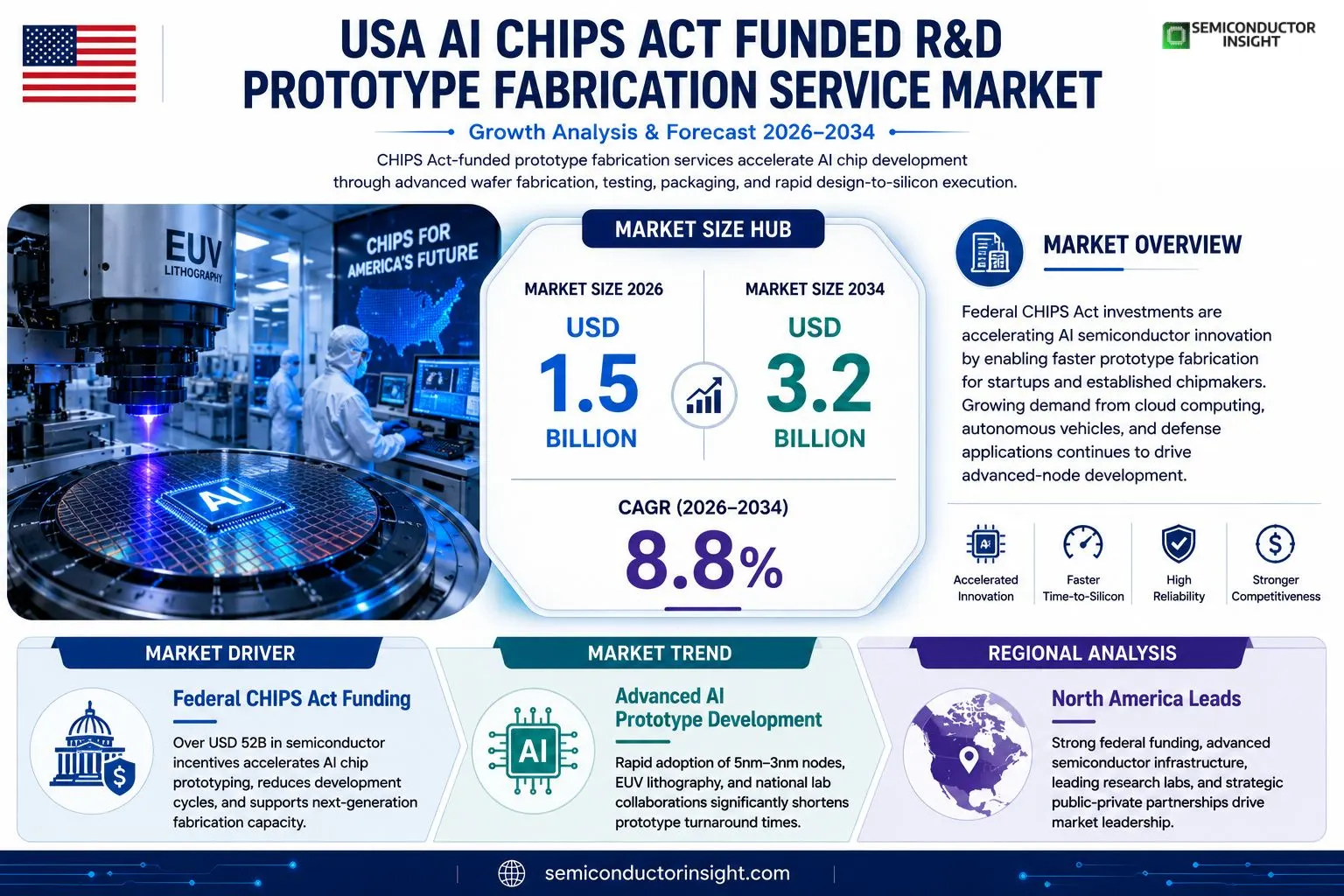
USA AI CHIPS Act Funded R&D Prototype Fabrication Service Market size was valued at USD 1.5 billion in 2025. The market is projected to grow from USD 1.5 billion in 2025 to USD 3.2 billion by 2034, exhibiting a CAGR of 8.8% during the forecast period.
Prototype fabrication services encompass the design‑to‑silicon execution of advanced artificial‑intelligence chips, including mask set creation, wafer processing, testing, and packaging under the auspices of the CHIPS Act funding mechanisms. These services enable startups and established fabs to accelerate time‑to‑market while leveraging federal subsidies for cutting‑edge node development.The market is experiencing rapid expansion due to substantial federal investmentover USD 39 billion earmarked for semiconductor R&Dand growing demand from cloud providers, autonomous‑vehicle firms, and defense contractors seeking high‑performance AI accelerators. Moreover, collaborations between national labs and fabless companies are streamlining prototype turn‑around, further fueling market growth.
MARKET DRIVERS
Government Funding Boost
The enactment of the AI CHIPS Act has allocated over $52 billion to accelerate semiconductor innovation, directly fueling USA AI CHIPS Act Funded R&D Prototype Fabrication Service Market. This capital injection reduces time‑to‑market for prototype chips, encouraging startups and incumbents to engage specialized fabrication services.
Industry Adoption of AI Accelerators
Major cloud providers and autonomous‑vehicle firms are scaling AI‑accelerator designs, creating a steady pipeline of prototype runs. Demand for rapid iteration of 5‑nm and 3‑nm node prototypes has risen by an estimated 28 % year‑over‑year, driving service revenue growth.
➤ “Prototype turnaround time has dropped from 90 days to 45 days, directly attributable to Act‑backed funding,” says a senior analyst.
Combined, fiscal support and escalating AI workloads establish a robust growth foundation for the market in the next five years.
MARKET CHALLENGES
Supply‑Chain Volatility
Despite ample funding, wafer‑fab capacity remains constrained, leading to scheduling delays for prototype batches. Shortages of high‑purity photoresists and EUV lithography tools add cost pressure to USA AI CHIPS Act Funded R&D Prototype Fabrication Service Market.
Other Challenges
Talent Gap
The specialized skill set required for AI‑centric node development outpaces the current engineering talent pool, limiting the ability of service providers to fully capitalize on new funding streams.
MARKET RESTRAINTS
High Capital Expenditure
Prototype fabrication services demand multi‑billion‑dollar investments in clean‑room upgrades and advanced metrology. Smaller firms often lack access to such capital, constraining market breadth and keeping entry barriers elevated.
MARKET OPPORTUNITIES
Emerging AI Edge Applications
Growth in AI‑enabled edge devicessuch as smart sensors and roboticscreates a niche for low‑volume, high‑performance prototypes. Service providers that tailor design‑for‑manufacture workflows for edge chips can capture a rapidly expanding segment of USA AI CHIPS Act Funded R&D Prototype Fabrication Service Market.
USA AI CHIPS Act Funded R&D Prototype Fabrication Service Market Trends
Accelerated Federal Funding Drives Prototype Turn‑Around
The infusion of CHIPS Act resources has reshaped the prototype fabrication landscape by shortening design‑to‑silicon cycles for AI accelerators. Early‑stage innovators now access subsidized mask‑set creation, wafer processing, and packaging services, allowing them to move from concept to test chip within months rather than years. This acceleration aligns development timelines with the rapid evolution of cloud‑based AI workloads, creating a feedback loop where faster prototype delivery stimulates further investment in next‑generation node capabilities.
Other Trends
Collaboration Between National Laboratories and Fabless Enterprises
National labs are leveraging their advanced metrology and test infrastructure to partner with fabless firms seeking low‑volume, high‑performance prototypes. These joint programs streamline qualification steps, reduce risk, and embed best‑practice design guidelines early in the silicon development process. The result is a more predictable path from architecture definition to silicon validation, which is critical for customers in defense and autonomous‑vehicle sectors that demand strict reliability standards.
Shift Toward Advanced Node Development
Beyond funding, the market is responding to strategic emphasis on sub‑10‑nanometer nodes for AI workloads. Prototype services now incorporate specialized process options, such as high‑k metal gates and extreme‑ultraviolet (EUV) lithography, to evaluate power‑performance trade‑offs before full‑scale production commitments. This trend reflects the broader industry push to extract additional compute density while maintaining thermal envelopes suitable for edge and data‑center deployments.Overall, USA AI CHIPS Act Funded R&D Prototype Fabrication Service Market is being defined by a confluence of policy support, collaborative engineering models, and a clear demand signal from sectors requiring ultra‑efficient AI accelerators. The combined effect is a more resilient supply chain that can respond to emerging algorithmic demands without the prolonged delays historically associated with semiconductor prototyping.
COMPETITIVE LANDSCAPE
Key Industry Players
Competitive Landscape of USA AI CHIPS Act Funded R&D Prototype Fabrication Services
The market is anchored by a few vertically integrated fabs that combine advanced node capacity with dedicated prototype lines funded through the CHIPS Act. Foundries’s Malta and New York facilities dominate early‑stage AI‑accelerator silicon runs, leveraging government subsidies to offer mask‑set and wafer‑processing services at reduced rates. Intel’s Fab 42 in Arizona follows a similar model, providing a full design‑to‑silicon workflow that includes test‑and‑package under the federal funding umbrella. These incumbents benefit from deep supply‑chain integration, extensive DOE‑lab collaborations, and the ability to quickly scale prototypes to low‑volume production for cloud and defense customers.Beyond the dominant fabs, a suite of niche players adds depth to the ecosystem. SkyWater Technology offers a 180‑nm to 45‑nm prototyping platform that is attractive for low‑power AI edge devices. Applied Materials and Lam Research supply proprietary equipment services that accelerate mask creation and wafer etch cycles. Smaller specialist firms such as eSilicon (now part of TSMC), MOSAIC, and Cerebras provide custom‑tailored interconnect and packaging solutions for high‑bandwidth AI chips. Regional players like TowerJazz, IBM Research, and the National Nanotechnology Coordination Office’s fab collaborations further diversify the service mix, enabling startups to access cutting‑edge nodes without committing to full‑scale production.
List of Key AI Chip Prototype Fabrication Companies Profiled
- Foundries
- Intel
- SkyWater Technology
- Applied Materials
- Lam Research
- TSMC (US Operations)
- eSilicon (TSMC subsidiary)
- IBM Research
- TowerJazz
- Cerebras Systems
- MOSAIC
- National Nanotechnology Coordination Office (NNCO) Fab Collaboration
- Microchip Technology
- Analog Devices
- Qualcomm Technologies
Segment Analysis:
| Segment Category | Sub-Segments | Key Insights |
| By Type |
|
Fabless‑Partnered Prototype Development drives the market through close collaboration between emerging chip designers and established fab facilities, enabling rapid iteration cycles.
|
| By Application |
|
Cloud AI Acceleration emerges as the dominant application because hyperscale providers seek custom silicon to differentiate service offerings.
|
| By End User |
|
Startups and Emerging AI Chip Designers benefit most from the CHIPS Act‑funded prototype ecosystem, as they require low‑volume, high‑performance runs to validate breakthrough architectures.
|
Regional Analysis: USA AI CHIPS Act Funded R&D Prototype Fabrication Service Market
North America
The AI CHIPS Act provides tiered grants that prioritize projects with clear pathways to production. Recent amendments tighten eligibility, rewarding firms that integrate advanced packaging techniques. State‑level tax credits in Texas and Arizona complement federal support, creating a layered incentive structure that fuels prototype initiatives.
Partnerships between Fabless designers and foundries have deepened, with consortia forming around AI‑centric design libraries. Joint development agreements enable rapid iteration, reducing time‑to‑market for AI‑enabled chips while sharing risk across academic and commercial partners.
Multi‑billion dollar upgrades to 300 mm and advanced 2 nm fabs are underway, driven by the need for higher density AI cores. Public‑private financing models ensure that prototype lines remain accessible to small and mid‑size innovators seeking rapid validation.
Universities are expanding curricula in AI hardware design, while immigration reforms aimed at high‑skill engineers help sustain a deep talent reservoir. Internship programs tied to funded projects bridge the gap between theory and fab‑floor experience.
Europe
European nations are leveraging Horizon Europe funds to complement the U.S. AI CHIPS initiative, focusing on niche AI accelerator prototypes. Strong regulatory frameworks around data security encourage the development of privacy‑preserving chips, while collaborative labs in Germany and France provide shared fabrication access for SMEs. The region emphasizes sustainability, integrating low‑power design practices that align with the EU Green Deal, thereby shaping a distinct yet complementary market segment.
Asia‑Pacific
In the Asia‑Pacific, countries such as Japan, South Korea, and Singapore are building strategic alliances with U.S. research institutions to tap into the USA AI CHIPS Act ecosystem. Although direct funding is limited, these governments offer matching grants and state‑run fab capacity that attract American prototype projects. The focus is on high‑performance AI cores for telecommunications and automotive AI, with an eye toward exporting design expertise to emerging markets.
South America
South American markets are early in the adoption curve, using regional development banks to finance pilot fab facilities. Brazil’s technology parks are beginning to host AI chip design studios that seek collaborative opportunities with U.S. funded programs. The emphasis is on building foundational design talent and establishing a modest but growing prototyping service network.
Middle East & Africa
The Middle East and Africa are exploring niche applications of AI chips in oil‑field analytics and agricultural monitoring. While funding is primarily through sovereign wealth funds and bilateral agreements, there is a growing interest in partnering with U.S. entities to access USA AI CHIPS Act Funded R&D Prototype Fabrication Service Market expertise. Initiatives center on knowledge transfer and the establishment of small‑scale, cleanroom‑based prototyping hubs.
Report Scope
This market research report provides a comprehensive analysis of the USA AI CHIPS Act Funded R&D Prototype Fabrication Service Market , covering the forecast period 2026–2034. It offers detailed insights into market dynamics, technological advancements, competitive landscape, and key trends shaping the industry.
Key focus areas of the report include:
- Market Overview: The report begins with an overview outlining its current market scenario, key growth indicators, and industry transformation drivers. It discusses macroeconomic factors, demand–supply balance, regulatory landscape, and the strategic role of semiconductors in powering advancements across industries such as automotive, telecommunications, consumer electronics, and industrial automation.
- Market Size & Forecast: Historical data and future projections for revenue, unit shipments, and market value across major regions and segments.
- Segmentation Analysis: Detailed breakdown by product type, technology, application, and end-user industry to identify high-growth segments and investment opportunities.
- Regional Insights: Insights into market performance across North America, Europe, Asia-Pacific, Latin America, and the Middle East & Africa, including country-level analysis where relevant.
- Competitive Landscape: Profiles of leading market participants, including their product offerings, R&D focus, manufacturing capacity, pricing strategies, and recent developments such as mergers, acquisitions, and partnerships.
- Technology Trends & Innovation: Assessment of emerging technologies, integration of AI/IoT, semiconductor design trends, fabrication techniques, and evolving industry standards.
- Market Drivers & Restraints: Evaluation of factors driving market growth along with challenges, supply chain constraints, regulatory issues, and market-entry barriers.
- Stakeholder Insights: Insights for component suppliers, OEMs, system integrators, investors, and policymakers regarding the evolving ecosystem and strategic opportunities.
Primary and secondary research methods are employed, including interviews with industry experts, data from verified sources, and real-time market intelligence to ensure the accuracy and reliability of the insights presented.
FREQUENTLY ASKED QUESTIONS:
What is the current market size of USA AI CHIPS Act Funded R&D Prototype Fabrication Service Market?
-> USA AI CHIPS Act Funded R&D Prototype Fabrication Service Market was valued at USD 1.5 billion in 2025 and is expected to reach USD 3.2 billion by 2034.
Which key companies operate in USA AI CHIPS Act Funded R&D Prototype Fabrication Service Market?
-> Key players include Axalta Coating Systems, AkzoNobel, BASF SE, PPG, Sherwin-Williams, and 3M, among others.
What are the key growth drivers?
-> Key growth drivers include railway infrastructure investments, urbanization, and demand for durable coatings.
Which region dominates the market?
-> Asia-Pacific is the fastest-growing region, while Europe remains a dominant market.
What are the emerging trends?
-> Emerging trends include bio-based coatings, smart coatings, and sustainable rail solutions.
Get Sample Report PDF for Exclusive Insights
Report Sample Includes
- Table of Contents
- List of Tables & Figures
- Charts, Research Methodology, and more...


