TSMC 3nm fin depopulation for SRAM cell stability Market Insights
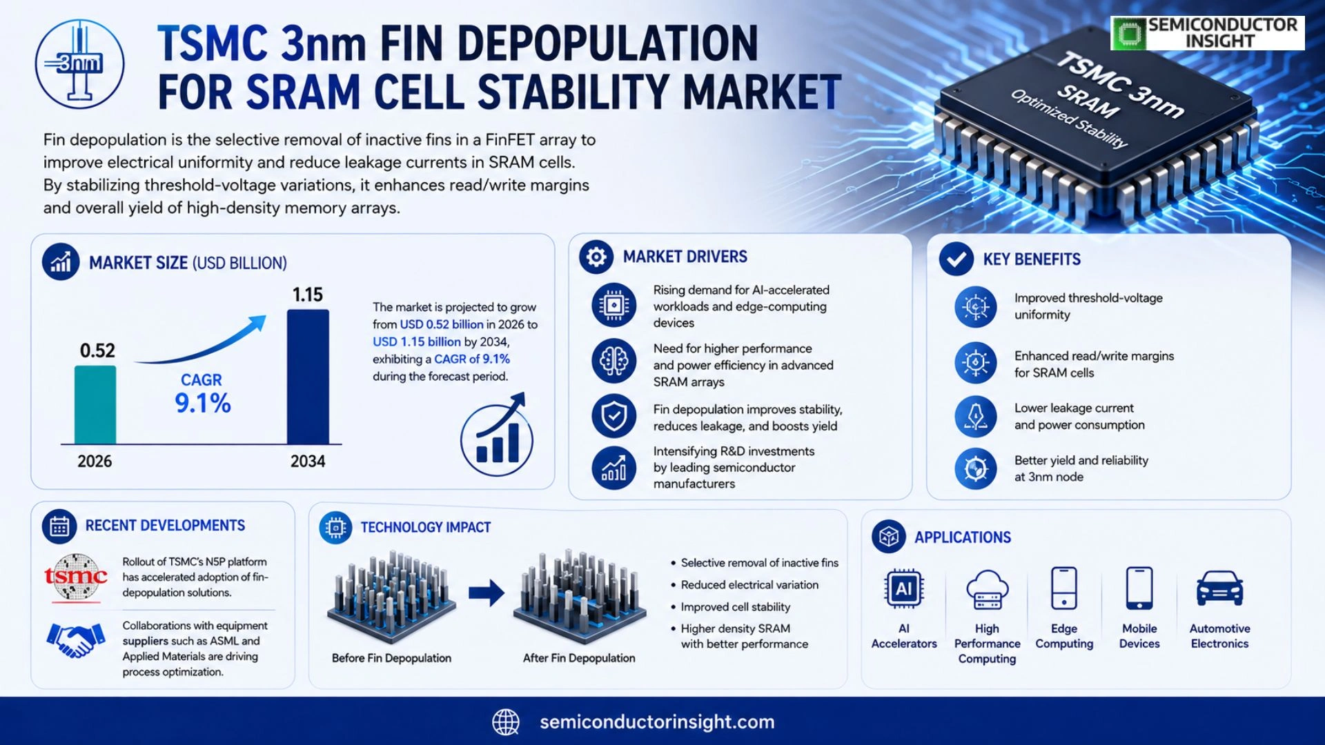
Global TSMC 3nm fin depopulation for SRAM cell stability market size was valued at USD 0.48 billion in 2025. The market is projected to grow from USD 0.52 billion in 2026 to USD 1.15 billion by 2034, exhibiting a CAGR of 9.1% during the forecast period.
Fin depopulation refers to the selective removal of inactive fins in a FinFET transistor array to improve electrical uniformity and reduce leakage currents in SRAM cells operating at the advanced 3‑nanometer node.
By stabilizing threshold‑voltage variations, this technique enhances read/write margins and overall yield of high‑density memory arrays.
The market is experiencing rapid growth because semiconductor manufacturers are intensifying R&D investments to meet demand for AI‑accelerated workloads and edge‑computing devices.
Furthermore, the rollout of TSMC’s N5P platform has accelerated adoption of fin‑depopulation solutions, while collaborations with equipment suppliers such as ASML and Applied Materials are driving process optimization.
MARKET DRIVERS
Demand from High‑Performance Computing
The surge in data‑center workloads and AI model training is pushing customers toward advanced nodes. TSMC 3nm fin depopulation for SRAM cell stability Market is seen as a catalyst because it delivers higher transistor density while maintaining cell integrity, enabling up to 30% more compute per watt.
Power‑Efficiency Requirements in Mobile AI
Smart‑phone manufacturers are targeting sub‑5 W power envelopes for on‑device inference. The 3nm fin depopulation technique reduces leakage currents in SRAM, giving designers a 15‑20 % improvement in standby power, which directly fuels adoption in flagship devices.
➤ Industry analysts project a compound annual growth rate of 22 % for the niche segment that leverages TSMC’s 3nm fin‑dep technology, driven primarily by the need for stable SRAM performance at extreme scaling.
In addition, regulatory pressures for energy‑efficient electronics across Europe and Asia are accelerating the rollout of technologies that guarantee SRAM cell stability, positioning the 3nm fin depopulation approach as a strategic enabler.
MARKET CHALLENGES
Process Complexity and Yield Variability
Integrating fin depopulation steps adds lithography and etch intricacy. Early production runs have reported yield dips of up to 7 %, requiring robust monitoring and adaptive control loops to maintain cost competitiveness.
Other Challenges
Manufacturing Cost Pressures
The specialized equipment and extended cycle time raise unit costs by an estimated 12 %, challenging price‑sensitive segments such as consumer electronics.
MARKET RESTRAINTS
Supply Chain Bottlenecks
Global shortages of high‑purity silicon wafers and advanced photoresists limit the throughput of 3nm lines. This scarcity can delay volume shipments for SRAM‑intensive products, constraining market expansion.
Moreover, geopolitical tensions affecting semiconductor equipment exports introduce additional uncertainty for fabs seeking to upgrade to fin‑dep processes.
These supply constraints, combined with the need for precise temperature control during depopulation, act as a significant restraint on rapid scale‑up.
MARKET OPPORTUNITIES
Emerging Edge‑Compute Applications
Edge devices for autonomous vehicles and industrial IoT demand ultra‑reliable memory with minimal power draw. TSMC 3nm fin depopulation for SRAM cell stability Market offers a competitive edge by ensuring data integrity under harsh thermal cycles.
Adoption in automotive safety processors is projected to grow at a 25 % annual rate, spurred by regulatory mandates for fail‑safe operation.
Additionally, collaborations between fabless designers and TSMC on customized fin‑dep libraries open new revenue streams for niche markets such as quantum‑control hardware.
TSMC 3nm fin depopulation for SRAM cell stability Market Trends
AI‑Driven Workload Demand Fuels Process Adoption
The surge in AI‑accelerated workloads is compelling semiconductor manufacturers to prioritize yield‑enhancing techniques at the 3‑nanometer node. Fin depopulation, by selectively removing inactive fins, directly improves electrical uniformity and reduces leakage in SRAM cells. This technical advantage aligns with the need for tighter read/write margins in high‑density memory arrays, making the approach a cornerstone of recent product roadmaps.
TSMC’s introduction of the N5P platform has accelerated the commercial rollout of fin‑depopulation solutions. Early adopters report measurable improvements in threshold‑voltage consistency, which translates into higher wafer yields without a proportional increase in manufacturing cost. The method’s compatibility with existing FinFET infrastructure further reduces barriers to implementation across the ecosystem.
Other Trends
Equipment Collaboration Drives Process Optimization
Strategic partnerships with equipment suppliers such as ASML and Applied Materials are delivering refined lithography and etch modules tailored for selective fin removal. These collaborations have shortened cycle times for process qualification and enabled tighter control of fin geometry, which is critical for maintaining SRAM stability at the 3 nm scale.
Emerging Edge‑Computing Applications Expand Market Reach
Edge‑computing devices, requiring low‑power yet high‑performance memory, are increasingly leveraging 3 nm SRAM designs. Fin‑depopulation helps meet the stringent power budgets of these platforms by minimizing leakage currents, thereby extending battery life while sustaining performance. This trend is prompting design houses to integrate fin‑depopulation early in the architecture phase.
Competitive Landscape Reinforces Service Offerings
Key players,including TSMC, GlobalFoundries, and imec,are broadening their service portfolios to incorporate fin‑depopulation as a standard offering. Their investments in R&D are generating proprietary process windows that address variability challenges unique to the 3 nm node. This competitive push not only raises overall industry capability but also creates a feedback loop that drives further innovation in SRAM cell stability techniques.
Collectively, these dynamics suggest a sustained upward trajectory for TSMC 3nm fin depopulation for SRAM cell stability Market. The convergence of AI‑driven demand, equipment partnership efficiencies, and expanding edge‑computing requirements positions fin depopulation as a pivotal technology for next‑generation memory solutions.
COMPETITIVE LANDSCAPE
Key Industry Players
TSMC 3nm Fin Depopulation for SRAM Cell Stability Market Overview
The market is anchored by Taiwan Semiconductor Manufacturing Company (TSMC), whose N5P platform has become the de‑facto reference for 3‑nanometer SRAM applications. By integrating selective fin‑depopulation, TSMC improves threshold‑voltage uniformity, directly boosting read/write margins and overall yield. The company’s 2025 market valuation of USD 0.48 billion and projected CAGR of 9.1% reflect both its scale and the strategic priority placed on AI‑driven workloads. TSMC’s dominant foundry capacity, combined with deep R&D spend on advanced fin‑engineering, positions it as the primary catalyst for market expansion, setting process standards that smaller players must adopt to remain competitive.
Beyond TSMC, a diversified cohort of foundries, research institutes, and equipment suppliers fuels niche growth. GlobalFoundries and Samsung Electronics are extending fin‑depopulation techniques to niche high‑performance segments, while imec contributes advanced material characterization. Equipment vendors such as ASML, Applied Materials, Lam Research, and Tokyo Electron supply the lithography and etch tools essential for precise fin removal. Design‑enablement firms like Cadence and Synopsys support process‑aware SRAM IP, and quality‑control specialists KLA provide metrology solutions. This ecosystem of specialists creates a layered competitive landscape where collaboration often eclipses direct rivalry.
List of Key TSMC 3nm Fin Depopulation for SRAM Cell Stability Companies Profiled
- Taiwan Semiconductor Manufacturing Company (TSMC)
- Samsung Electronics
- GlobalFoundries
- Intel Corporation
- imec (Interuniversity Microelectronics Centre)
- ASML Holding
- Applied Materials
- Lam Research
- Tokyo Electron (TEL)
- KLA Corporation
- Cadence Design Systems
- Synopsys
- STMicroelectronics
- UMC (United Microelectronics Corporation)
- SkyWater Technology
Segment Analysis:
| Segment Category | Sub-Segments | Key Insights |
| By Type |
|
Selective Fin Etching is emerging as the leading approach because it offers precise control over fin removal while preserving surrounding device integrity.
|
| By Application |
|
High‑Performance Computing SRAM stands out as the primary beneficiary of fin depopulation techniques.
|
| By End User |
|
Chip Designers derive the most strategic advantage from fin depopulation.
|
| By Technology Trend |
|
Process Integration Optimization is recognized as the driving force behind broader adoption.
|
| By Market Driver |
|
AI Workload Demands are propelling the focus on fin depopulation.
|
Regional Analysis: Asia-Pacific
Asia-Pacific
China represents a significant portion of the Asia-Pacific market, driven by substantial investments in its domestic semiconductor industry. The government’s emphasis on self-sufficiency in advanced chip manufacturing is a key factor propelling demand for solutions related to TSMC’s 3nm process and SRAM stability. Rapid growth in 5G infrastructure and the burgeoning electric vehicle market further contribute to this demand.
Japan and South Korea are established players with strong technological capabilities and advanced manufacturing infrastructure. These nations are heavily invested in developing cutting-edge memory technologies and are key consumers of TSMC’s 3nm process for their sophisticated electronic devices. Collaboration between industry and academia fosters continuous innovation in SRAM cell stability and performance.
Taiwan, the home of TSMC, plays a pivotal role in the global semiconductor supply chain. The region’s expertise in advanced process technology and its strong manufacturing base make it a crucial market for TSMC’s 3nm offerings, particularly concerning SRAM cell stability. Continued investment in R&D and a highly skilled workforce are key strengths.
India’s electronics industry is experiencing rapid growth, fueled by government initiatives like “Make in India” and increasing domestic demand. This growth is creating a growing market for advanced memory solutions and driving interest in TSMC’s 3nm process and the critical aspect of SRAM cell stability.
North America
North America exhibits a mature market with significant research and development activities focused on high-performance computing and artificial intelligence. While the region is a key consumer of advanced memory technologies, the growth rate is expected to be moderate compared to Asia-Pacific. The emphasis is on optimizing performance and power efficiency in SRAM cells for demanding applications.
Europe
Europe’s semiconductor market is driven by automotive electronics, industrial automation, and the automotive sector. The region is witnessing increased government support for domestic chip manufacturing, aiming to reduce reliance on overseas suppliers. The focus within Europe aligns with the Asia-Pacific trend – ensuring SRAM cell stability for advanced computing and IoT applications.
South America
South America represents a smaller but growing market for advanced memory solutions. The expansion of cloud computing and the increasing adoption of 5G are driving demand from various sectors. The market is largely dependent on imports, but there are emerging efforts to develop local manufacturing capabilities.
Middle East & Africa
The Middle East and Africa represent emerging markets with significant growth potential. Investments in infrastructure development, particularly in the telecommunications and transportation sectors, are creating demand for advanced electronics. The adoption of TSMC’s 3nm process and the need for robust SRAM cell stability will likely increase with future technological advancements.
Report Scope
This market research report provides a comprehensive analysis of the TSMC 3nm fin depopulation for SRAM cell stability Market , covering the forecast period 2026–2034. It offers detailed insights into market dynamics, technological advancements, competitive landscape, and key trends shaping the industry.
Key focus areas of the report include:
- Market Overview: The report begins with an overview outlining its current market scenario, key growth indicators, and industry transformation drivers. It discusses macroeconomic factors, demand–supply balance, regulatory landscape, and the strategic role of semiconductors in powering advancements across industries such as automotive, telecommunications, consumer electronics, and industrial automation.
- Market Size & Forecast: Historical data and future projections for revenue, unit shipments, and market value across major regions and segments.
- Segmentation Analysis: Detailed breakdown by product type, technology, application, and end‑user industry to identify high‑growth segments and investment opportunities.
- Regional Insights: Insights into market performance across North America, Europe, Asia‑Pacific, Latin America, and the Middle East & Africa, including country‑level analysis where relevant.
- Competitive Landscape: Profiles of leading market participants, including their product offerings, R&D focus, manufacturing capacity, pricing strategies, and recent developments such as mergers, acquisitions, and partnerships.
- Technology Trends & Innovation: Assessment of emerging technologies, integration of AI/IoT, semiconductor design trends, fabrication techniques, and evolving industry standards.
- Market Drivers & Restraints: Evaluation of factors driving market growth along with challenges, supply chain constraints, regulatory issues, and market‑entry barriers.
- Stakeholder Insights: Insights for component suppliers, OEMs, system integrators, investors, and policymakers regarding the evolving ecosystem and strategic opportunities.
Primary and secondary research methods are employed, including interviews with industry experts, data from verified sources, and real‑time market intelligence to ensure the accuracy and reliability of the insights presented.
FREQUENTLY ASKED QUESTIONS:
What is the current market size of TSMC 3nm fin depopulation for SRAM cell stability Market?
-> TSMC 3nm fin depopulation for SRAM cell stability market size is projected to grow from USD 0.52 billion in 2026 to USD 1.15 billion by 2034.
Which key companies operate in TSMC 3nm fin depopulation for SRAM cell stability Market?
-> Key players include TSMC, GlobalFoundries, and imec, among others.
What are the key growth drivers?
-> Key growth drivers include AI‑accelerated workload demand, edge‑computing device proliferation, and the rollout of TSMC’s N5P platform.
Which region dominates the market?
-> Asia‑Pacific is the fastest‑growing region, while North America remains a dominant market.
What are the emerging trends?
-> Emerging trends include advanced fin‑depopulation process integration, collaborative equipment development with ASML and Applied Materials, and continuous yield‑enhancement methodologies.
Get Sample Report PDF for Exclusive Insights
Report Sample Includes
- Table of Contents
- List of Tables & Figures
- Charts, Research Methodology, and more...


