MARKET INSIGHTS
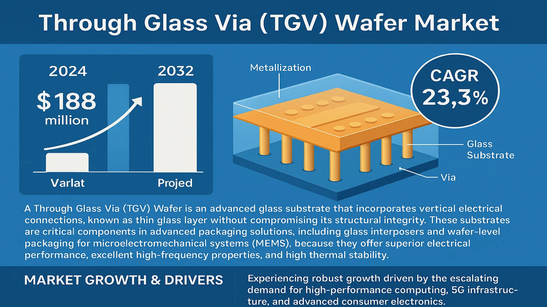
The global Through Glass Via (TGV) Wafer Market was valued at 188 million in 2024 and is projected to reach US$ 848 million by 2032, at a CAGR of 23.3% during the forecast period.
A Through Glass Via (TGV) Wafer is an advanced glass substrate that incorporates vertical electrical connections, known as vias, which are created through a thin glass layer without compromising its structural integrity. These substrates are critical components in advanced packaging solutions, including glass interposers and wafer-level packaging for microelectromechanical systems (MEMS), because they offer superior electrical performance, excellent high-frequency properties, and high thermal stability.
The market is experiencing robust growth driven by the escalating demand for high-performance computing, 5G infrastructure, and advanced consumer electronics. The United States is the dominant market, holding approximately 46% of the global share, while Europe follows with about 25%. The competitive landscape is relatively concentrated, with Corning leading the market and accounting for 26% of the global production value. Other key players such as LPKF (11%) and Samtec (10%) are also significant contributors, alongside companies like Kiso Micro Co. LTD and Tecnisco.
MARKET DYNAMICS
MARKET DRIVERS
Growing Demand for Advanced Semiconductor Packaging to Drive Market Expansion
The global semiconductor industry’s relentless pursuit of miniaturization and performance enhancement is significantly driving the adoption of Through Glass Via (TGV) wafers. These substrates enable higher integration density and superior electrical performance compared to traditional organic or silicon-based interposers, making them indispensable for advanced packaging solutions. The market is witnessing substantial growth because TGV technology supports higher input/output densities and offers excellent high-frequency characteristics, which are critical for 5G, artificial intelligence, and high-performance computing applications. With the semiconductor advanced packaging market projected to exceed $50 billion by 2027, the demand for TGV wafers as a key enabling technology continues to accelerate across multiple high-growth sectors.
Expansion of MEMS and Sensor Applications to Boost Market Growth
The proliferation of microelectromechanical systems (MEMS) and sensor technologies across consumer electronics, automotive, and medical devices represents a major growth driver for TGV wafers. These substrates provide exceptional hermetic sealing properties and thermal stability, making them ideal for sensitive MEMS devices that require protection from environmental factors. The automotive sector’s increasing adoption of MEMS sensors for advanced driver assistance systems (ADAS) and the medical industry’s growing use of implantable devices have created substantial demand for reliable packaging solutions. With the global MEMS market expected to reach approximately $40 billion by 2028, TGV wafers are becoming increasingly essential for next-generation device packaging that demands higher reliability and performance standards.
Superior Material Properties Over Conventional Substrates to Fuel Adoption
TGV wafers offer distinct advantages over silicon and organic substrates, including lower electrical loss, better high-frequency performance, and enhanced thermal management capabilities. These material properties are particularly valuable in radio frequency applications where signal integrity is paramount. The technology’s ability to provide excellent insulation properties reduces cross-talk between adjacent vias, enabling higher integration densities without compromising performance. Furthermore, glass substrates exhibit coefficient of thermal expansion values that closely match those of many semiconductor materials, reducing mechanical stress and improving device reliability. These technical advantages are driving increased adoption across telecommunications infrastructure, where 5G deployment requires components capable of operating at millimeter-wave frequencies with minimal signal degradation.
Additionally, recent manufacturing innovations have improved TVD wafer production efficiency, with several leading manufacturers achieving production yields exceeding 85% for 200mm wafers, making the technology increasingly commercially viable for high-volume applications.
MARKET RESTRAINTS
High Manufacturing Costs and Complex Production Processes to Limit Market Penetration
The production of Through Glass Via wafers involves sophisticated manufacturing techniques including laser drilling, etching, and metallization processes that require significant capital investment and operational expertise. The specialized equipment needed for creating high-aspect-ratio vias in glass substrates represents a substantial barrier to entry, with complete production lines costing upwards of $20 million. Additionally, the materials themselves, particularly high-quality borosilicate glass, contribute to higher production costs compared to conventional silicon wafers. These cost factors make TGV wafers approximately 30-40% more expensive than equivalent silicon interposers, limiting their adoption to applications where their technical advantages justify the premium pricing.
Technical Challenges in Via Formation and Metallization to Hinder Widespread Adoption
Creating reliable electrical connections through glass substrates presents significant technical challenges that restrain market growth. The process of forming vias with high aspect ratios while maintaining glass structural integrity requires precise control of laser parameters and etching conditions. Metallization processes must ensure complete via filling without voids while achieving good adhesion to the glass surface, which is particularly challenging given glass’s inert nature. Variations in via geometry and metallization quality can lead to yield losses and reliability concerns, especially as via diameters shrink below 50 micrometers to meet the demands of advanced packaging applications. These technical hurdles require ongoing research and development investments, slowing the pace of commercialization and limiting the technology’s immediate market penetration.
Limited Standardization and Supply Chain Immaturity to Constrain Market Development
The TGV wafer market faces constraints due to the absence of established industry standards and a mature supply ecosystem. Unlike silicon interposers, which benefit from decades of manufacturing optimization and standardized processes, TGV technology lacks universally accepted specifications for via dimensions, pitch, and metallization approaches. This standardization gap creates interoperability concerns and increases development costs for end-users who must design specifically for available TGV solutions. Furthermore, the limited number of qualified manufacturers capable of producing high-volume, high-quality TGV wafers creates supply chain vulnerabilities and reduces competitive pressure that would otherwise drive cost reductions. The market’s relative immaturity means that many potential users perceive adoption risks that delay investment decisions despite the technology’s demonstrated technical advantages.
MARKET CHALLENGES
Scaling Production While Maintaining Quality Presents Significant Operational Challenges
As demand for TGV wafers increases, manufacturers face the dual challenge of scaling production capacity while maintaining stringent quality standards. The transition from laboratory-scale production to high-volume manufacturing requires overcoming substantial technical hurdles related to process control and yield optimization. Variations in glass material properties, laser drilling consistency, and metallization uniformity become increasingly difficult to manage at industrial scales, potentially leading to yield fluctuations that impact profitability. The industry must develop more robust process controls and advanced metrology techniques to ensure consistent performance across production batches, particularly as applications move toward smaller via diameters and higher integration densities that push the limits of current manufacturing capabilities.
Other Challenges
Thermal Management Considerations
While glass substrates offer excellent electrical properties, their thermal conductivity is lower than silicon, creating challenges for heat dissipation in high-power applications. Managing thermal performance requires innovative design approaches and sometimes additional thermal management features that increase complexity and cost. This thermal limitation restricts TGV adoption in certain power electronics applications where efficient heat removal is critical to device reliability and performance.
Integration with Existing Manufacturing Infrastructure
The semiconductor industry’s extensive investment in silicon processing infrastructure creates inertia against adopting alternative substrate technologies. Integrating TGV wafers into established fabrication flows requires modifications to handling equipment, process recipes, and quality assurance protocols. This integration challenge is particularly pronounced for companies with significant legacy investments in silicon processing, creating resistance to technology adoption despite potential performance benefits.
MARKET OPPORTUNITIES
Emerging Applications in Photonics and Quantum Computing to Create New Growth Frontiers
The unique properties of glass substrates present significant opportunities in emerging technology sectors, particularly integrated photonics and quantum computing. TGV wafers provide an excellent platform for photonic integrated circuits due to glass’s transparency at optical wavelengths and its ability to form waveguides and optical interfaces. The global integrated photonics market is projected to grow substantially as demand increases for optical communication technologies in data centers and telecommunications infrastructure. Similarly, quantum computing applications benefit from glass substrates’ low electrical loss and ability to provide stable, low-noise environments for qubit operation. These emerging applications represent potential market expansion opportunities beyond traditional semiconductor packaging, potentially doubling the addressable market for advanced glass substrate technologies within the next decade.
Advancements in Manufacturing Technologies to Enable Cost Reduction and Market Expansion
Ongoing developments in laser processing, etching techniques, and metallization methods are creating opportunities for significant cost reductions and performance improvements in TGV wafer production. New laser sources with higher repetition rates and improved beam quality are increasing via formation speeds while reducing thermal damage to the glass substrate. Advanced etching chemistries are enabling higher aspect ratios with improved profile control, while novel metallization approaches are improving via filling efficiency and electrical performance. These manufacturing advancements are expected to reduce production costs by approximately 25-30% over the next five years, making TGV technology more competitive with established packaging solutions and enabling expansion into cost-sensitive market segments.
Strategic Collaborations and Vertical Integration to Accelerate Technology Adoption
The formation of strategic partnerships between glass manufacturers, equipment suppliers, and semiconductor companies presents significant opportunities for market growth. These collaborations enable knowledge sharing, technology transfer, and coordinated development efforts that accelerate innovation and reduce time-to-market for new TGV-based products. Several major semiconductor companies have recently established development partnerships with glass substrate manufacturers to co-develop customized TGV solutions for specific application requirements. Additionally, vertical integration strategies, where glass manufacturers expand into value-added processing services, are creating more complete solution offerings that simplify adoption for end customers. These collaborative approaches are reducing barriers to entry and creating more robust ecosystem support for TGV technology adoption across multiple industry sectors.
THROUGH GLASS VIA (TGV) WAFER MARKET TRENDS
Advanced Packaging and Miniaturization Driving Market Expansion
The relentless push towards device miniaturization and enhanced performance in the semiconductor and electronics industries is fundamentally driving the adoption of Through Glass Via (TGV) wafers. These substrates are critical for creating high-density interconnects in advanced packaging solutions like 2.5D and 3D integrated circuits. Glass, as a substrate material, offers superior electrical properties, including excellent insulation and low signal loss at high frequencies, which is paramount for 5G and RF applications. Furthermore, its coefficient of thermal expansion is closely matched to silicon, reducing stress and increasing reliability in multi-chip packages. This trend is accelerating as the industry moves beyond traditional silicon interposers to meet the demanding performance and form factor requirements of next-generation consumer electronics, high-performance computing, and telecommunications infrastructure. The market is responding with increased production capacity and technological refinements in via formation and metallization processes to support this growing demand.
Other Trends
Biomedical and Life Sciences Applications
While consumer electronics is a primary driver, the biomedical and life sciences sector is emerging as a significant and high-growth application area for TGV wafers. The inherent properties of glass, such as its bio-inertness, optical transparency, and ability to be fabricated into complex microfluidic structures, make it an ideal platform for advanced medical devices. TGV wafers are increasingly being used in bio-MEMS, lab-on-a-chip devices, and implantable medical sensors. These applications require hermetically sealed, miniaturized components with reliable electrical feedthroughs, a need perfectly addressed by TGV technology. The integration of sensors and fluidic channels on a single glass substrate enables the development of sophisticated point-of-care diagnostic tools and continuous health monitoring systems, opening a substantial new market segment beyond traditional electronics.
Geographic Market Concentration and Competitive Landscape
The global TGV wafer market exhibits a distinct geographic concentration, with the United States holding a dominant position, accounting for approximately 46% of the market share. This leadership is largely attributed to the presence of major technology corporations, robust R&D infrastructure, and significant investments in advanced semiconductor packaging within the region. Europe follows as the second-largest market, contributing about 25% of global share, supported by strong automotive and industrial electronics sectors. The competitive landscape is relatively concentrated, with a few key players leading technological development and production. Corning Inc. maintains a commanding presence, holding an estimated 26% of the global production value market share, leveraging its deep expertise in glass science. Other significant participants, including LPKF and Samtec, hold shares of approximately 21% and 11%, respectively. This concentration suggests high barriers to entry due to the sophisticated technology and capital-intensive nature of TGV wafer manufacturing.
COMPETITIVE LANDSCAPE
Key Industry Players
Technological Innovation and Strategic Expansion Drive Market Leadership
The global Through Glass Via (TGV) Wafer market exhibits a semi-consolidated competitive structure, characterized by a mix of established multinational corporations and specialized technology firms. Corning Incorporated dominates the market, holding approximately 26% of the global production value share in 2024. This leadership position is primarily attributed to its proprietary fusion draw process, which enables the production of ultra-thin, pristine glass substrates essential for high-performance TGV applications. The company’s extensive R&D investments, which exceeded $1 billion annually in recent years, and its strong relationships with major semiconductor and consumer electronics companies have solidified its market dominance.
LPKF Laser & Electronics AG and Samtec Inc. are also significant players, collectively accounting for approximately 32% of market share. LPKF’s strength lies in its laser-based via formation technologies, which offer precision and scalability for high-volume manufacturing. The company’s recent partnership with a major Asian foundry has expanded its production capacity significantly. Meanwhile, Samtec has leveraged its expertise in high-speed interconnect solutions to develop advanced TGV-based packaging for 5G and automotive applications, capturing valuable market segments.
These leading companies are actively pursuing growth through both organic innovation and strategic acquisitions. Corning’s recent expansion of its Harrodsburg, Kentucky facility specifically for advanced glass packaging solutions demonstrates the industry’s commitment to meeting growing demand. Similarly, LPKF’s acquisition of a laser technology specialist in 2023 has enhanced its capabilities in glass processing, positioning the company for increased market penetration.
Emerging players including Kiso Micro Co. LTD, Tecnisco, and Microplex are focusing on niche applications and specialized technologies to differentiate themselves. These companies are particularly active in developing TGV solutions for medical devices and aerospace applications, where reliability and precision are paramount. Their growth strategies often involve partnerships with research institutions and targeted technology licensing agreements to accelerate market entry.
List of Key Through Glass Via (TGV) Wafer Companies Profiled
- Corning Incorporated (U.S.)
- LPKF Laser & Electronics AG (Germany)
- Samtec Inc. (U.S.)
- Kiso Micro Co. LTD (Japan)
- Tecnisco (Japan)
- Microplex (Germany)
- Plan Optik AG (Germany)
- NSG Group (Japan)
- Allvia Inc. (U.S.)
- Xiamen Sky Semiconductor Technology (China)
Segment Analysis:
By Type
300 mm Wafer Segment Dominates the Market Due to Superior Manufacturing Efficiency and High-Volume Production Demands
The market is segmented based on type into:
- 300 mm
- 200 mm
- Below 150 mm
By Application
Consumer Electronics Segment Leads Due to Proliferation of Advanced RF Components and High-Performance MEMS Devices
The market is segmented based on application into:
- Biotechnology/Medical
- Consumer Electronics
- Automotive
- Others
By End User
Semiconductor Foundries and IDMs Lead the Market Due to High Adoption in Advanced Packaging and Interposer Applications
The market is segmented based on end user into:
- Semiconductor Foundries & IDMs
- MEMS Manufacturers
- Research & Development Institutes
- OSATs (Outsourced Semiconductor Assembly and Test Providers)
By Glass Type
Borosilicate Glass Segment Holds Significant Share Due to its Excellent Thermal and Mechanical Properties for TGV Fabrication
The market is segmented based on glass type into:
- Borosilicate Glass
- Fused Silica/Quartz
- Soda-Lime Glass
- Others
Regional Analysis: Through Glass Via (TGV) Wafer Market
North America
The North American region, led by the United States which holds approximately 46% of the global market share, is the dominant force in the TGV wafer industry. This leadership is driven by substantial investments in advanced semiconductor packaging, robust R&D activities from leading technology firms, and strong demand from the consumer electronics and biotechnology sectors. The presence of key market players like Corning and Samtec, coupled with supportive government initiatives for technological innovation, creates a highly conducive environment for growth. The region’s focus on developing high-performance computing and next-generation MEMS devices ensures sustained demand for advanced TGV wafers, particularly in the 300 mm segment.
Europe
Europe is a significant follower in the global TGV wafer market, accounting for about 25% of market share. The region’s strength lies in its strong automotive industry, which is increasingly integrating advanced semiconductor components for electric and autonomous vehicles, and a well-established biotechnology/medical device sector. Countries like Germany, France, and the Nordic nations are at the forefront, driven by stringent quality standards and a focus on precision engineering. However, the market’s expansion is somewhat tempered by the high cost of advanced manufacturing and complex regulatory landscapes, though ongoing research in institutions and corporations continues to push the boundaries of TGV applications.
Asia-Pacific
The Asia-Pacific region represents the fastest-growing market for TGV wafers, fueled by massive electronics manufacturing hubs in China, South Korea, and Japan. This growth is propelled by the region’s dominance in consumer electronics production, increasing adoption of electric vehicles, and significant government and private investments in semiconductor self-sufficiency. While cost sensitivity leads to a higher volume demand for 200 mm and below 150 mm wafers, there is a clear and accelerating trend toward adopting more advanced 300 mm TGV solutions to meet the requirements of high-performance applications. The region is also becoming a hotbed for new entrants and expanding production capacities from established global players.
South America
The TGV wafer market in South America is in a nascent stage of development. Growth potential exists, primarily linked to the gradual modernization of industrial and technological infrastructure in countries like Brazil and Argentina. However, the market faces significant headwinds due to economic volatility, which limits capital expenditure on advanced semiconductor technologies, and a relatively underdeveloped local electronics manufacturing ecosystem. Adoption is currently restricted to niche applications and imports, with limited local production or significant investment from major global TGV wafer suppliers.
Middle East & Africa
This region is an emerging market with very limited current penetration of TGV wafer technology. Development is isolated to specific nations with targeted economic diversification and technology investment strategies, such as Israel, Turkey, and the UAE. While these countries show interest in building high-tech industries, the overall market growth is constrained by a lack of a foundational semiconductor ecosystem, limited specialized manufacturing capabilities, and funding priorities directed elsewhere. Long-term potential hinges on sustained investment and the development of local technological hubs, but widespread adoption is not anticipated in the immediate future.
Report Scope
This market research report provides a comprehensive analysis of the global and regional Semiconductor and Electronics markets, covering the forecast period 2025–2032. It offers detailed insights into market dynamics, technological advancements, competitive landscape, and key trends shaping the industry.
Key focus areas of the report include:
- Market Size & Forecast: Historical data and future projections for revenue, unit shipments, and market value across major regions and segments.
- Segmentation Analysis: Detailed breakdown by product type, technology, application, and end-user industry to identify high-growth segments and investment opportunities.
- Regional Outlook: Insights into market performance across North America, Europe, Asia-Pacific, Latin America, and the Middle East & Africa, including country-level analysis where relevant.
- Competitive Landscape: Profiles of leading market participants, including their product offerings, R&D focus, manufacturing capacity, pricing strategies, and recent developments such as mergers, acquisitions, and partnerships.
- Technology Trends & Innovation: Assessment of emerging technologies, integration of AI/IoT, semiconductor design trends, fabrication techniques, and evolving industry standards.
- Market Drivers & Restraints: Evaluation of factors driving market growth along with challenges, supply chain constraints, regulatory issues, and market-entry barriers.
- Stakeholder Analysis: Insights for component suppliers, OEMs, system integrators, investors, and policymakers regarding the evolving ecosystem and strategic opportunities.
Primary and secondary research methods are employed, including interviews with industry experts, data from verified sources, and real-time market intelligence to ensure the accuracy and reliability of the insights presented.
FREQUENTLY ASKED QUESTIONS:
What is the current market size of Global Through Glass Via (TGV) Wafer Market?
-> Through Glass Via (TGV) Wafer Market was valued at 188 million in 2024 and is projected to reach US$ 848 million by 2032, at a CAGR of 23.3% during the forecast period.
Which key companies operate in Global Through Glass Via (TGV) Wafer Market?
-> Key players include Corning, LPKF, Samtec, Kiso Micro Co.LTD, Tecnisco, Microplex, Plan Optik, NSG Group, Allvia, and Xiamen Sky Semiconductor Technology, among others.
What are the key growth drivers?
-> Key growth drivers include demand for advanced packaging in consumer electronics, growth in MEMS applications, and increasing adoption in biotechnology/medical devices.
Which region dominates the market?
-> North America is the dominant market, with the United States holding approximately 46% market share, while Europe follows with about 25%.
What are the emerging trends?
-> Emerging trends include integration with AI-driven manufacturing, development of larger 300mm wafers, and expansion into automotive and 5G applications.

Get Sample Report PDF for Exclusive Insights
Report Sample Includes
- Table of Contents
- List of Tables & Figures
- Charts, Research Methodology, and more...