Thick Film Cavity SOI Wafer Market Market Insights
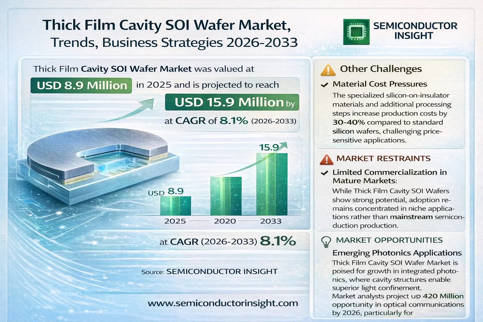
Global Thick Film Cavity SOI Wafer Market was valued at USD 8.9 million in 2025 and is projected to reach USD 15.9 million by 2033, exhibiting a CAGR of 8.1% during the forecast period.
Thick Film Cavity SOI Wafer Market are specialized silicon-on-insulator substrates featuring deep cavities or recesses in the device layer, primarily used for MEMS (Micro-Electro-Mechanical Systems), sensors, and advanced semiconductor applications. These wafers enable the integration of microstructures, optical components, and pressure-sensitive devices while leveraging the benefits of SOI technology, such as reduced parasitic capacitance and improved performance.
The market growth is driven by increasing demand for high-performance semiconductors in 5G infrastructure, automotive electronics, and medical devices. For instance, cavity SOI substrates offer approximately 22% lower insertion loss in RF filters compared to traditional bulk silicon, making them critical for next-generation communication systems. Key players like Okmetic dominate the market with an 86% revenue share in 2025, reflecting high industry concentration.
MARKET DRIVERS
Growing Demand for High-Performance RF Applications
Thick Film Cavity SOI Wafer Market is driven by increasing adoption in 5G infrastructure, where these wafers enable superior RF performance. Their low-loss characteristics make them ideal for power amplifiers and RF switches in mobile devices and base stations. The market is projected to grow at 8.2% CAGR through 2027 as telecom operators expand 5G networks globally.
Advancements in Semiconductor Manufacturing
Improved fabrication techniques for Thick Film Cavity SOI Wafer Market have reduced production costs by approximately 15% over the past three years. Semiconductor manufacturers are investing heavily in specialized etching and deposition technologies to enhance wafer quality and yield rates. This has expanded their use in automotive radar and IoT applications.
Automotive electrification trends are further driving demand, as these wafers provide the thermal stability required for electric vehicle power management systems.
Thick Film Cavity SOI Wafer Market MARKET CHALLENGES
High Production Complexity
Manufacturing Thick Film Cavity SOI Wafer Market requires precise control over cavity dimensions and film thickness, leading to yield rates 10-15% lower than conventional SOI wafers. This production complexity limits supply chain scalability despite growing demand.
Other Challenges
Material Cost Pressures
The specialized silicon-on-insulator materials and additional processing steps increase production costs by 30-40% compared to standard silicon wafers, challenging price-sensitive applications.
Thick Film Cavity SOI Wafer Market MARKET RESTRAINTS
Limited Commercialization in Mature Markets
While Thick Film Cavity SOI Wafer Market show strong potential, adoption remains concentrated in niche applications rather than mainstream semiconductor production. Only 18% of foundries currently offer dedicated production lines for these specialized wafers.
Thick Film Cavity SOI Wafer Market MARKET OPPORTUNITIES
Emerging Photonics Applications
Thick Film Cavity SOI Wafer Market is poised for growth in integrated photonics, where cavity structures enable superior light confinement. Market analysts project a USD 420 million opportunity in optical communications by 2026, particularly for data center interconnects and LiDAR systems.
Thick Film Cavity SOI Wafer Market Trends
Growth Trajectory and Market Valuation
Global Thick Film Cavity SOI Wafer Market was valued at USD 8.9 million in 2025, with projections indicating growth to USD 15.9 million by 2033 at a CAGR of 8.1%. This expansion is driven by increasing demand across advanced communication, automotive, and consumer electronics sectors. The market remains highly concentrated, with the top three manufacturers holding approximately 98% of revenue share, led by Okmetic at 86%.
Other Trends
Technological Advancements in 5G Infrastructure
Thick Film Cavity SOI Wafer Market are critical for 5G networks, offering 22% lower insertion loss in RF filters compared to traditional silicon. This efficiency enhancement supports the rapid deployment of ultra-low-loss components in advanced communication systems worldwide.
Expansion in Automotive Electronics
The rise of ADAS and autonomous driving technologies has substantially increased semiconductor requirements. Cavity SOI wafers provide the necessary performance and reliability for these applications, positioning them as a key enabler for next-generation vehicle systems.
Regional Market Developments
Asia dominates the Thick Film Cavity SOI Wafer Market, accounting for the largest revenue share due to robust electronics manufacturing. North America and Europe follow, with significant investments in MEMS and sensor technologies driving regional demand. Emerging markets show potential as production capabilities expand globally.
Supply Chain and Competitive Landscape
With only four major manufacturers Okmetic, SEIREN KST, IceMOS Technology, and PlutoSemi supply remains tightly controlled. Geopolitical factors and tariff policies influence market dynamics, necessitating strategic planning for resilient supply chains.
COMPETITIVE LANDSCAPE
Key Industry Players
Okmetic Dominates with 86% Market Share in High-Concentration Thick Film Cavity SOI Wafer Space
Thick Film Cavity SOI Wafer Market exhibits extreme concentration with Finland’s Okmetic controlling 86% of global revenues as of 2025. The top three players collectively account for 98% market share, establishing a near-oligopoly structure. These specialty wafers require advanced MEMS manufacturing capabilities and proprietary cavity forming technologies, creating high barriers for new entrants. Okmetic’s dominance stems from its vertically integrated production facilities and strategic partnerships with automotive MEMS sensor manufacturers.
Niche competitors like IceMOS Technology and SEIREN KST focus on specific applications such as RF filters for 5G infrastructure and medical MEMS devices. Japan’s SEIREN KST has gained traction in optical MEMS applications through its proprietary deep reactive ion etching (DRIE) technology. Emerging players like PlutoSemi are investing in 200mm wafer capabilities to address growing demand from autonomous vehicle sensor manufacturers, though face challenges in achieving production-scale yields.
List of Key Thick Film Cavity SOI Wafer Companies Profiled
- Okmetic Oy
- IceMOS Technology
- SEIREN KST Corporation
- PlutoSemi Technology
- SOITEC SA
- Silicon Nexus Solutions
- MEMSCAP Inc.
- EV Group (EVG)
- Tower Semiconductor
- Silex Microsystems
- Nanosilicon Inc.
- Rogue Valley Microdevices
- Ultratech (Veeco)
- Adesto Technologies
- X-FAB Silicon Foundries
Segment Analysis:
| Segment Category | Sub-Segments | Key Insights |
| By Type |
|
200mm Wafers dominate due to:
|
| By Application |
|
RF Components show strongest growth potential due to:
|
| By End User |
|
Automotive Sector demonstrates strongest adoption due to:
|
| By Technology Sophistication |
|
Deep Cavity SOI gains traction due to:
|
| By Manufacturing Process |
|
Smart Cut Technology emerges as preferred method because:
|
Regional Analysis: Global Thick Film Cavity SOI Wafer Market
Asia-Pacific
Asia-Pacific leads in developing novel cavity structures with improved thermal dissipation characteristics. Regional players have pioneered integration techniques that combine thick film deposition with cavity isolation for high-frequency applications.
The region boasts complete vertical integration for thick film cavity SOI wafers, from raw material suppliers to specialized equipment manufacturers. This ecosystem reduces lead times and enables customization for specific end-use applications.
Asian research institutions and corporate R&D centers are filing numerous patents related to cavity SOI architectures. Collaborative projects between universities and foundries accelerate technology transfers for thick film applications.
Local demand from smartphone manufacturers, automotive Tier 1 suppliers, and telecom infrastructure providers creates a strong pull for advanced thick film cavity SOI solutions tailored to regional technical requirements.
North America
North America maintains strong positions in thick film cavity SOI wafer design and high-end applications, particularly for defense and aerospace sectors. The region benefits from close collaboration between fabless semiconductor companies and specialty foundries. Research institutions are developing novel cavity-based SOI solutions for quantum computing and advanced sensor applications. California’s semiconductor ecosystem plays a pivotal role in developing thick film processes optimized for RF front-end modules.
Europe
European players specialize in thick film cavity SOI wafers for automotive and industrial applications, with Germany and France leading development efforts. The region has seen growing adoption in MEMS-based pressure sensors and power management ICs. EU-funded research initiatives support advancements in cavity wafer reliability and thermal management. Local manufacturers focus on quality consistency and stringent automotive-grade certifications for their thick film offerings.
Middle East & Africa
While currently a smaller market, the region shows growing interest in thick film cavity SOI technologies for telecommunications infrastructure. Emerging semiconductor initiatives in countries like Israel and the UAE are exploring cavity wafer applications. Local demand primarily stems from oil & gas sensing equipment and next-generation base station deployments requiring robust RF components.
South America
Thick Film Cavity SOI Wafer Market remains nascent but shows potential in Brazil’s growing electronics manufacturing sector. Local universities are establishing research programs focusing on MEMS applications using cavity wafers. Limited local production capabilities currently lead to dependency on imports, though some regional assembly of SOI-based modules is emerging.
Report Scope
This market research report provides a comprehensive analysis of the Thick Film Cavity SOI Wafer Market, covering the forecast period 2025–2033. It offers detailed insights into market dynamics, technological advancements, competitive landscape, and key trends shaping the industry.
Key focus areas of the report include:
- Market Overview: The report begins with an overview outlining its current market scenario, key growth indicators, and industry transformation drivers. It discusses macroeconomic factors, demand–supply balance, regulatory landscape, and the strategic role of semiconductors in powering advancements across industries such as automotive, telecommunications, consumer electronics, and industrial automation.
- Market Size & Forecast: Historical data and future projections for revenue, unit shipments, and market value across major regions and segments.
- Segmentation Analysis: Detailed breakdown by product type, technology, application, and end-user industry to identify high-growth segments and investment opportunities.
- Regional Insights: Insights into market performance across North America, Europe, Asia-Pacific, Latin America, and the Middle East & Africa, including country-level analysis where relevant.
- Competitive Landscape: Profiles of leading market participants, including their product offerings, R&D focus, manufacturing capacity, pricing strategies, and recent developments such as mergers, acquisitions, and partnerships.
- Technology Trends & Innovation: Assessment of emerging technologies, integration of AI/IoT, semiconductor design trends, fabrication techniques, and evolving industry standards.
- Market Drivers & Restraints: Evaluation of factors driving market growth along with challenges, supply chain constraints, regulatory issues, and market-entry barriers.
- Stakeholder Insights: Insights for component suppliers, OEMs, system integrators, investors, and policymakers regarding the evolving ecosystem and strategic opportunities.
Primary and secondary research methods are employed, including interviews with industry experts, data from verified sources, and real-time market intelligence to ensure the accuracy and reliability of the insights presented.
FREQUENTLY ASKED QUESTIONS:
What is the current market size of Thick Film Cavity SOI Wafer Market?
-> Thick Film Cavity SOI Wafer Market was valued at USD 8.9 million in 2025 and is projected to reach USD 15.9 million by 2033, exhibiting a CAGR of 8.1% during the forecast period.
Which key companies operate in Thick Film Cavity SOI Wafer Market?
-> Key players include Okmetic, SEIREN KST, IceMOS Technology, and PlutoSemi. Okmetic dominates with 86% revenue share in 2025.
What are the key growth drivers?
-> Key growth drivers include 5G network rollout (22% lower RF insertion loss), ADAS/autonomous vehicle adoption, and medical device miniaturization.
Which region dominates the market?
-> Asia holds significant market share, with key demand from China, Japan, and South Korea.
What are the emerging trends?
-> Emerging trends include MEMS integration, advanced semiconductor applications, and cavity SOI technology innovations.
Get Sample Report PDF for Exclusive Insights
Report Sample Includes
- Table of Contents
- List of Tables & Figures
- Charts, Research Methodology, and more...
 Download Sample Report PDF