
Single-Photon Avalanche Photodiode (SPAD) Market Insights
Single-Photon Avalanche Photodiode (SPAD) market size was valued at USD 284 million in 2026. The market is projected to grow from USD 284 million in 2026 to USD 566 million by 2034, exhibiting a CAGR of 10.7% during the forecast period.
The Single‑Photon Avalanche Diode (SPAD) operates in Geiger mode, where a reverse‑bias voltage exceeds the breakdown threshold and a single photon initiates an ionisation avalanche that produces a measurable current pulse. This mechanism enables detection of individual photons with picosecond timing resolution and delivers a binary “click” output that eliminates the need for external low‑noise amplification.
Market expansion reflects rising adoption of three‑dimensional sensing modules and automotive‑grade LiDAR systems across Asia, particularly China’s fast‑growing manufacturing base. Advances in hybrid‑bonding and three‑dimensional stacking further lower dark‑count rates while supporting pixel pitches below 10 µm, opening opportunities in short‑wave infrared LiDAR and quantum‑communication links. Leading suppliers such as STMicroelectronics, Hamamatsu, Sony Semiconductor Solutions, Onsemi and Excelitas have announced new BSI‑SPAD product families or strategic investments aimed at scaling volume production and enhancing performance for automotive and industrial applications.
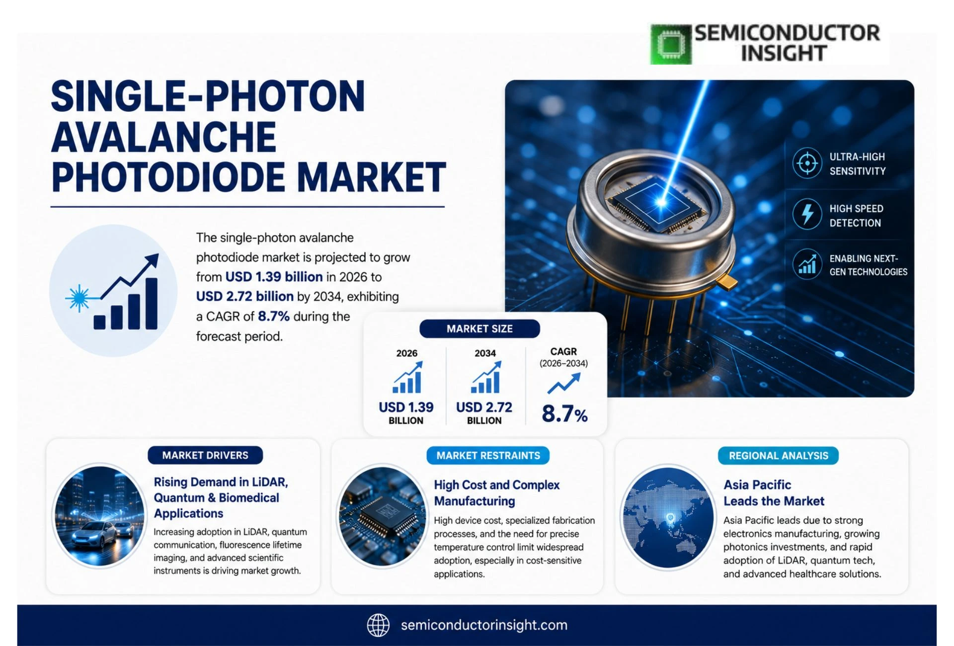
MARKET DRIVERS
Expansion of Autonomous‑Vehicle Sensing
The shift toward driverless platforms has intensified the need for precise range‑finding sensors. **Single-Photon Avalanche Photodiode (SPAD) Market** participants are benefiting from manufacturers integrating SPAD arrays into lidar modules, where single‑photon sensitivity translates into longer detection distances while keeping power consumption low.
Rise of Quantum‑Enabled Imaging
Research labs and defense contractors are experimenting with quantum‑illumination techniques that rely on the ultra‑low noise performance of SPAD devices. The ability to discriminate single photons against background radiation makes these detectors attractive for secure imaging and low‑light surveillance, prompting a noticeable uptick in procurement budgets.
➤ “Adoption of SPAD technology in time‑correlated single‑photon counting is reshaping biomedical fluorescence lifetime imaging, delivering sub‑nanosecond resolution that was previously unattainable.”
Medical diagnostics firms are therefore allocating capital to embed SPAD sensors in portable fluorescence devices, a move that promises faster assay turnaround and opens new revenue streams beyond traditional industrial applications.
MARKET CHALLENGES
Manufacturing Yield Constraints
Silicon‑based SPAD structures demand tight control over doping profiles and isolation trenches. Even minor variations can cause premature breakdown, resulting in lower usable die counts. **Manufacturers** consequently face higher per‑unit costs, which can limit price competitiveness against alternative photodetectors.
Other Challenges
Thermal Management
Operating SPAD arrays at high frame rates generates localized heating. Without effective cooling solutions, dark‑count rates rise sharply, eroding the detector’s signal‑to‑noise advantage and compelling system designers to incorporate additional thermal hardware.
MARKET RESTRAINTS
Regulatory Hurdles in Medical Devices
Approval processes for diagnostic equipment that embed SPAD sensors are lengthy and resource‑intensive. Health‑authority filings often require extensive clinical validation, which can delay market entry and deter smaller innovators lacking regulatory expertise.
MARKET OPPORTUNITIES
Integration with Integrated‑Photonic Platforms
Emerging silicon‑photonic foundries now offer co‑fabrication of waveguides and SPAD detectors on a single chip. This convergence lowers assembly steps, reduces footprint, and enables mass‑production of compact Lidar and quantum‑communication modules, presenting a clear growth pathway for firms that can leverage such turnkey processes.
Single-Photon Avalanche Photodiode (SPAD) Market Trends
Asian Manufacturing Ascendancy
The production footprint of the Single-Photon Avalanche Photodiode (SPAD) Market is recalibrating toward East Asia. China’s capacity share is projected to eclipse half of global output, propelled by the rollout of domestic 12‑inch 3D‑Stack + InGaAs‑NFAD lines. This scale‑up lowers unit cost for volume‑oriented designs while preserving the high‑performance edge required in LiDAR and quantum‑communication modules. Meanwhile, established players in Japan and the United States retain niche advantages in materials expertise and precision processes, but their relative contribution to total shipments is slowly receding. For downstream OEMs, the geographic shift translates into shorter lead times and greater negotiating leverage, yet it also introduces supply‑chain concentration risks that must be mitigated through diversified sourcing strategies.
Other Trends
SWIR Segment Gains Momentum
Short‑Wave Infrared (SWIR) SPADs are moving from a peripheral specialty to a core revenue driver. The rise of 1550 nm flash/FMCW LiDAR systems and emerging quantum‑key‑distribution links pushes demand for detectors that combine low dark‑count rates with high photon‑conversion efficiency. Manufacturers are responding with wafer‑scale integration and price‑tiered product families that retain the premium performance needed for long‑range sensing while gradually eroding the cost gap with traditional visible–NIR devices. This evolution reshapes the value chain, encouraging semiconductor fabs to invest in mixed‑material process modules and prompting system integrators to redesign optical architectures around the narrower spectral window.
Automotive Applications Become Dominant Driver
The automotive sector is reshaping the demand profile of the Single-Photon Avalanche Photodiode (SPAD) Market. Adoption of high‑resolution 3D‑sensing arrays for advanced driver‑assistance systems fuels a sustained uptick in unit volumes, and the segment’s share of total sales is poised to surpass a quarter of the market by the early 2030s. This trajectory compels component suppliers to qualify devices against automotive reliability standards, accelerate temperature‑compensation schemes, and embed on‑chip timing circuitry to meet stringent latency requirements. Companies that align product roadmaps with automotive qualification cycles are likely to secure long‑term contracts, whereas those lagging in ruggedization may find their market relevance diminishing as OEMs consolidate around compliant sources.
COMPETITIVE LANDSCAPE
Key Industry Players
Single‑Photon Avalanche Photodiode (SPAD) Market – Competitive Overview
STMicroelectronics dominates the high‑volume segment, leveraging its 300 mm CMOS fabs in Europe to supply Si‑SPAD arrays for automotive LiDAR and consumer 3‑D sensing. The company’s integrated SoC approach, combining SPAD pixels with on‑chip TDCs, creates a barrier for newcomers because it ties design cycles to the semiconductor roadmap. Chinese manufacturers, fortified by recent 12‑inch 3‑D‑Stack lines, are rapidly closing the gap in unit production, yet they still rely on foreign IP for advanced BSI‑SPAD processes. In North America, a handful of specialty foundries maintain niche footholds in InGaAs‑based devices for quantum communication, preserving a fragmented but technologically diverse supply base.
Beyond the market leader, several specialists shape the ecosystem. Hamamatsu Photonics supplies premium VIS/NIR SPAD modules that underpin scientific instrumentation, while Onsemi focuses on ruggedized automotive‑grade parts with elevated breakdown voltages. Excelitas offers hybrid‑bonded SPAD‑CMOS solutions targeting SWIR applications, and Sony Semiconductor Solutions distinguishes itself with high‑yield BSI‑SPAD production in the Kumamoto facility. Smaller innovators such as Micro Photon Devices, Adaps Photonics, Laser Components, Runmingyu Electronics Technology, and CSEM contribute differentiated technologies—ranging from 10 µm pixel arrays to multi‑threshold counting ASICs—thereby expanding the option set for system integrators seeking performance‑specific trade‑offs.
List of Key SPAD Companies Profiled
- STMicroelectronics
- Hamamatsu Photonics
- On Semiconductor (Onsemi)
- Excelitas Technologies
- Micro Photon Devices
- Sony Semiconductor Solutions
- Laser Components
- Adaps Photonics
- Runmingyu Electronics Technology
- CSEM
- PicoQuant
- TE Connectivity
Segment Analysis:
| Segment Category | Sub-Segments | Key Insights |
| By Type |
|
Visible Light remains the volume driver because it aligns with legacy imaging and consumer‑electronics architectures. – Manufacturers prioritize integration of visible‑light SPADs into CMOS image sensors, enabling compact, low‑cost designs. – Product road‑maps emphasize scaling pixel pitch below 10 µm to support high‑resolution depth sensing. – The maturity of silicon processing ensures reliable yield and consistent dark‑count performance, reinforcing market adoption. |
| By Application |
|
Automotive is emerging as the leading growth application due to rapid adoption of LiDAR‑based driver‑assist and autonomous systems. – System architects value the picosecond timing resolution of SPADs for accurate 3‑D mapping. – Integration of SPAD arrays with on‑chip TDCs simplifies module design, reducing BOM complexity. – The shift toward 1550 nm SWIR LiDAR is prompting hybrid‑bonding approaches that preserve high detection efficiency while meeting eye‑safety regulations. |
| By End User |
|
Automotive OEMs drive specifications toward rugged, high‑reliability SPAD solutions. – OEMs demand integrated SoC designs that embed SPADs, on‑chip histogramming, and AI‑enabled signal processing. – Qualification cycles emphasize temperature compensation and low dark‑count performance across wide operating ranges. – Partnerships with semiconductor foundries accelerate adoption of 300 mm CMOS platforms for large‑scale production. |
| By Material |
|
Si‑SPAD dominates because of its compatibility with mature silicon fabs and cost‑effective scaling. – Silicon enables aggressive pixel shrinkage and seamless integration with digital processing blocks. – Continuous improvements in surface passivation reduce dark‑count rates, enhancing reliability for long‑term deployments. – The material’s broad market base supports cross‑industry standardization, reinforcing ecosystem growth. |
| By Spectral Range |
|
Visible Light retains the largest addressable market because it serves legacy imaging, LIDAR, and consumer devices. – The industry is transitioning from single‑point SPADs to area‑array configurations, unlocking new use‑cases in gesture recognition. – Emerging hybrid‑bonding techniques allow visible‑light devices to incorporate auxiliary functions such as on‑chip TDC histograms. – Continued investment in wafer‑scale integration ensures that price pressures are mitigated while performance improves. |
Regional Analysis: Single-Photon Avalanche Photodiode (SPAD) Market
North America
Automotive lidar suppliers and medical‑imaging firms have integrated SPAD arrays into next‑generation sensors, leveraging their picosecond timing to improve depth resolution. The shift from proof‑of‑concept to volume production reflects a maturation of design‑for‑manufacturability practices that reduce yield losses. As manufacturers embed SPADs into OEM platforms, supply chains become more resilient, encouraging downstream OEM investment.
Federal programs such as the National Quantum Initiative and Defense Advanced Research Projects Agency (DARPA) allocate multi‑year grants specifically for photon‑counting technologies. These funds complement private‑sector Series A and B rounds, creating a financing continuum that supports both exploratory research and scale‑up phases without the typical hiatus that stalls many niche markets.
The region benefits from a geographically concentrated semiconductor ecosystem, where wafer fabs, assembly houses, and test facilities coexist within a few hours’ drive. This proximity shortens lead times for custom SPAD processes and enables rapid iteration cycles, a competitive edge over more fragmented global supply networks.
Harmonized standards across the United States and Canada streamline product certification for medical and defense applications. Clear pathways for compliance reduce time to market, allowing developers to focus resources on performance enhancements rather than regulatory navigation.
Europe
European research consortia, particularly those anchored in Germany and the Netherlands, have cultivated a collaborative environment for SPAD development. Public–private partnerships blend academic discovery with industrial scaling, feeding niches such as quantum‑key‑distribution and high‑resolution spectroscopy. While the market size lags behind North America, Europe’s emphasis on sustainability and precision instrumentation drives demand for low‑power, high‑efficiency detectors. Regulatory frameworks that prioritize data security and privacy further incentivize domestic manufacturers to embed SPAD solutions in telecommunications hardware, reinforcing a self‑sufficient supply chain across the continent.
Asia‑Pacific
The Asia‑Pacific region presents a dynamic growth trajectory, propelled by aggressive investment in photonic foundries across China, Japan, and South Korea. Manufacturing capacity is expanding at a pace that enables cost‑effective production of larger SPAD arrays, appealing to consumer‑electronics firms seeking depth‑sensing capabilities for smartphones and wearables. Simultaneously, governmental initiatives targeting quantum research create a pipeline of talent that feeds both upstream device engineering and downstream system integration. Cultural emphasis on rapid market entry translates into shorter product lifecycles, compelling global players to engage with local partners to stay relevant.
South America
In South America, Brazil and Chile are emerging as modest hubs for SPAD research, largely linked to university laboratories focusing on biomedical imaging. Limited domestic fabrication infrastructure pushes firms to rely on imports, yet this dependency encourages the formation of niche service providers specializing in device testing and calibration. Regional health initiatives that prioritize early disease detection drive interest in photon‑counting technologies, creating a modest yet meaningful demand base that could attract foreign investment seeking untapped markets.
Middle East & Africa
The Middle East & Africa region currently exhibits a nascent SPAD ecosystem, with activity concentrated in a handful of research institutes in the United Arab Emirates and South Africa. Governmental diversification strategies, particularly those aimed at building a knowledge‑based economy, have allocated modest funding toward photonic sensor research. While large‑scale manufacturing remains absent, the region’s strategic positioning between Europe and Asia offers potential as a testing ground for field‑deployed SPAD applications in security and remote‑sensing projects, laying groundwork for future market entry.
Report Scope
This market research report provides a comprehensive analysis of the Single-Photon Avalanche Photodiode (SPAD) Market , covering the forecast period 2026–2034. It offers detailed insights into market dynamics, technological advancements, competitive landscape, and key trends shaping the industry.
Key focus areas of the report include:
-
Market Overview: The report begins with an overview outlining its current market scenario, key growth indicators, and industry transformation drivers. It discusses macroeconomic factors, demand–supply balance, regulatory landscape, and the strategic role of semiconductors in powering advancements across industries such as automotive, telecommunications, consumer electronics, and industrial automation.
- Market Size & Forecast: Historical data and future projections for revenue, unit shipments, and market value across major regions and segments.
- Segmentation Analysis: Detailed breakdown by product type, technology, application, and end-user industry to identify high-growth segments and investment opportunities.
- Regional Insights: Insights into market performance across North America, Europe, Asia-Pacific, Latin America, and the Middle East & Africa, including country-level analysis where relevant.
- Competitive Landscape: Profiles of leading market participants, including their product offerings, R&D focus, manufacturing capacity, pricing strategies, and recent developments such as mergers, acquisitions, and partnerships.
- Technology Trends & Innovation: Assessment of emerging technologies, integration of AI/IoT, semiconductor design trends, fabrication techniques, and evolving industry standards.
- Market Drivers & Restraints: Evaluation of factors driving market growth along with challenges, supply chain constraints, regulatory issues, and market-entry barriers.
- Stakeholder Insights: Insights for component suppliers, OEMs, system integrators, investors, and policymakers regarding the evolving ecosystem and strategic opportunities.
Primary and secondary research methods are employed, including interviews with industry experts, data from verified sources, and real-time market intelligence to ensure the accuracy and reliability of the insights presented.
FREQUENTLY ASKED QUESTIONS:
What is the current market size of Single-Photon Avalanche Photodiode (SPAD) Market?
-> The Single-Photon Avalanche Photodiode (SPAD) Market was valued at USD 284 million in 2026 and is expected to reach USD 566 million by 2034, representing a CAGR of 10.7% during the forecast period.
Which key companies operate in Single-Photon Avalanche Photodiode (SPAD) Market?
-> Key players include STMicroelectronics, Adaps Photonics, Hamamatsu, Onsemi, Excelitas, Micro Photon Devices, Sony Semiconductor Solutions, Laser Components, Runmingyu Electronics Technology, among others.
What are the key growth drivers?
-> Key growth drivers include the rapid expansion of 3D sensing and automotive‑grade LiDAR, increasing demand for short‑wave infrared (SWIR) solutions in quantum communications, and strong automotive sector investments driving double‑digit adoption rates.
Which region dominates the market?
-> Asia‑Pacific, led by China, is the fastest‑growing region and is projected to become the largest single‑consumer market, surpassing North America and Europe.
What are the emerging trends?
-> Emerging trends include 3D‑Stack and hybrid bonding technologies, pixel size reduction below 10 µm, AI‑ISP integration, multi‑threshold counting, and the migration of InGaAs/Ge‑on‑Si processes to 300 mm CMOS platforms.

Get Sample Report PDF for Exclusive Insights
Report Sample Includes
- Table of Contents
- List of Tables & Figures
- Charts, Research Methodology, and more...






