Silicon photonic chip for optical interconnects in HPC Market Insights
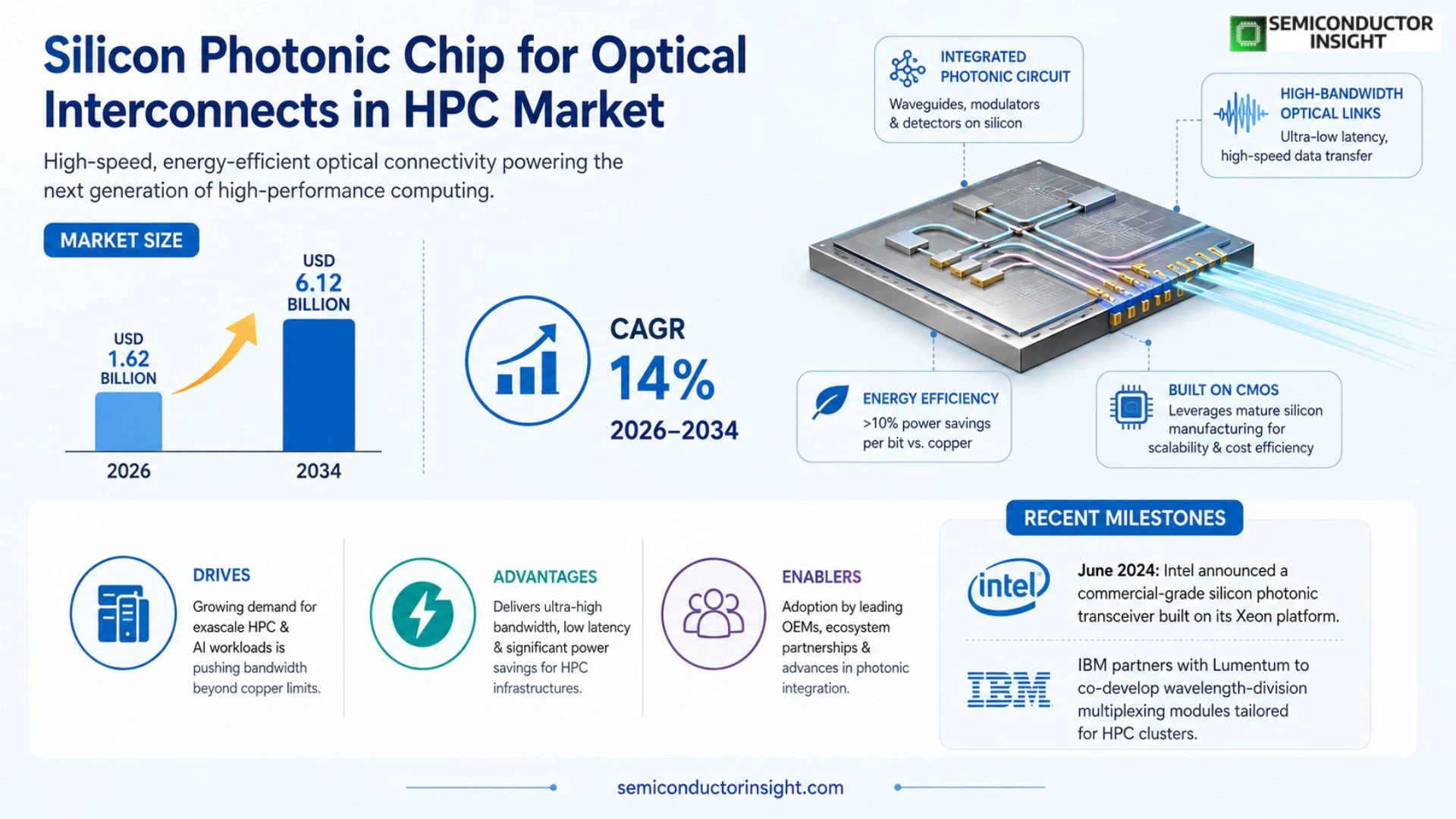
Global Silicon photonic chip for optical interconnects in HPC market size was valued at USD 1.85 billion in 2025. The market is projected to grow from USD 1.95 billion in 2025 to USD 6.12 billion by 2034, exhibiting a CAGR of 14 % during the forecast period.
Silicon photonic chips integrate optical waveguides, modulators and detectors on a single silicon substrate, enabling ultra‑high‑bandwidth optical interconnects that replace traditional copper links within high‑performance computing (HPC) clusters. By leveraging mature CMOS manufacturing, these chips deliver low‑latency data transmission while dramatically reducing power consumption compared with electrical alternatives.
The market is experiencing rapid growth because demand for exascale supercomputers and AI‑driven workloads is pushing data‑center bandwidth beyond the limits of copper wiring. Furthermore, energy‑efficiency targets,often exceeding 10 % power savings per bit,are driving adoption of silicon photonics across leading OEMs such as Intel, IBM and Cisco. Recent milestones include Intel’s announcement (June 2024) of a commercial‑grade silicon photonic transceiver built on its Xeon platform and IBM’s partnership with Lumentum to co‑develop wavelength‑division multiplexing modules tailored for HPC clusters.
MARKET DRIVERS
Rising Data‑Center Bandwidth Demands
The exponential growth of AI workloads and scientific simulations is pushing data‑center bandwidth requirements beyond 400 Gb/s per link. Silicon photonic chip for optical interconnects in HPC Market offers a scalable solution that can meet these throughput levels while maintaining low power consumption.
Energy‑Efficiency Imperatives
Traditional copper interconnects consume up to 30 % more power than comparable optical links. Silicon photonics reduces energy per bit to sub‑femtojoule levels, delivering significant OPEX savings for hyperscale operators.
➤ Integration of CMOS‑compatible photonic components accelerates time‑to‑market for new HPC platforms, enabling rapid adoption of next‑generation compute architectures.
Vendor roadmaps now highlight co‑packaged photonic transceivers, further simplifying system design and shortening deployment cycles.
MARKET CHALLENGES
Manufacturing Yield Variability
Achieving consistent high‑yield in sub‑micron silicon waveguide fabrication remains a technical hurdle, especially as feature sizes approach the 45 nm node. Yield gaps translate into higher unit costs for early adopters.
Other Challenges
Standardization Gaps
The absence of universally accepted optical interconnect standards for HPC creates integration friction, requiring custom engineering for each deployment.
Furthermore, the limited pool of skilled photonic design engineers slows the scaling of production capacity, impacting overall market momentum.
MARKET RESTRAINTS
Capital Expenditure Constraints
Data‑center operators face tight CapEx budgets, and the upfront cost of photonic transceiver modules,often 2‑3× higher than copper equivalents,acts as a barrier to large‑scale investment despite long‑term savings.
In addition, legacy infrastructure based on mature electrical interconnects requires extensive retrofitting to accommodate optical solutions, further restraining adoption rates.
MARKET OPPORTUNITIES
Emerging Co‑Design Initiatives
Collaboration between leading HPC vendors and silicon photonics foundries is unlocking co‑designed ASIC‑photonic platforms that promise to halve latency and double bandwidth density. These joint projects are expected to boost market penetration over the next five years.
Policy incentives for energy‑efficient computing in major economies also create a favorable environment for the adoption of optical interconnects, positioning silicon photonics as a strategic enabler for sustainable HPC growth.
Silicon photonic chip for optical interconnects in HPC Market Trends
Shift to Optical Interconnects for Exascale Computing
The adoption of silicon photonic chip for optical interconnects in HPC Market is accelerating as system architects confront the bandwidth limits of copper cabling. By integrating waveguides, modulators and photodetectors on a single silicon substrate, these chips enable terabit‑per‑second links with latency comparable to electrical alternatives. The pressure originates from exascale supercomputers and AI‑driven workloads that require sustained, high‑throughput data movement while keeping power consumption below stringent data‑center limits. Early deployments have demonstrated power savings of more than ten percent per transmitted bit, reinforcing the case for a wholesale transition to photonic interconnects.
Other Trends
CMOS‑Based Manufacturing Scale
Mature CMOS processes are the cornerstone of the current growth phase. Leveraging established silicon‑foundry infrastructure allows manufacturers to produce photonic components at volumes and costs previously unattainable for optics‑only solutions. The result is a supply chain that can meet the demand of large‑scale HPC clusters without compromising yield or reliability. Major OEMs such as Intel and IBM have integrated photonic layers directly into their Xeon‑class CPUs, delivering turnkey solutions that simplify system design and reduce the overall bill of materials. Energy‑efficiency improvements, driven by the low‑loss nature of silicon waveguides, continue to push the technology toward broader adoption.
Strategic Alliances and Product Roadmaps
Collaboration among leading vendors is sharpening the competitive edge of silicon photonics in the HPC arena. Intel’s 2024 announcement of a commercial‑grade silicon photonic transceiver, IBM’s partnership with Lumentum on wavelength‑division multiplexing modules, and Cisco’s integration of Acacia Communications’ coherent optics are illustrative of a coordinated push toward standardized, high‑performance solutions. These alliances accelerate R&D cycles, enable rapid feature integration, and provide customers with a predictable upgrade path as data‑center bandwidth requirements continue to climb. The combined effect of joint engineering programs and shared silicon roadmaps is a faster transition from prototype to production‑ready interconnects across the global HPC ecosystem.
COMPETITIVE LANDSCAPE
Key Industry Players
Silicon Photonic Chip Competitive Landscape for HPC Optical Interconnects
Silicon photonic ecosystem for high‑performance computing (HPC) is anchored by a few dominant silicon foundries that couple mature CMOS processes with advanced photonic device integration. Intel Corp. leads the market with its commercial‑grade silicon photonic transceiver line launched in June 2024, leveraging Xeon server platforms to deliver sub‑nanosecond latency and multi‑terabit per second bandwidth. IBM Corp. complements Intel’s offering through strategic collaborations with Lumentum Holdings on wavelength‑division multiplexing (WDM) modules that target exascale supercomputers. Cisco Systems Inc. focuses on data‑center back‑plane solutions, integrating silicon photonic links into its high‑density networking switches to meet the escalating bandwidth demand of AI workloads. Collectively, these leaders shape a market structure where large‑scale silicon fab capacity, deep R&D investment, and robust IP portfolios create high entry barriers, while also driving standardization around common optical form factors and interconnect protocols.
Beyond the tier‑one manufacturers, a vibrant tier‑two and niche segment fuels specialized capabilities and rapid innovation. Acacia Communications (now part of Cisco) provides high‑speed coherent transceivers that enhance long‑reach HPC cluster interconnects. Broadcom Inc. and Ciena Corporation supply optical aggregation chips and programmable photonic switches that improve scalability. Infinera Corporation and NeoPhotonics focus on integrated photonic engines for densely packed WDM solutions. Mellanox Technologies (NVIDIA) leverages silicon photonics to augment its InfiniBand products, while Xilinx (AMD) explores programmable silicon photonic ASICs for customizable HPC workloads. These players contribute differentiated device libraries, cost‑effective packaging, and niche market adoption that collectively broaden the competitive landscape and accelerate the transition from copper to silicon‑based optical interconnects.
List of Key Silicon Photonic Chip for Optical Interconnects in HPC Companies Profiled
- Intel Corp.
- Intel Corp.
- IBM Corp.
- IBM Corp.
- Lumentum Holdings Inc.
- Lumentum Holdings Inc.
- Cisco Systems Inc.
- Cisco Systems Inc.
- Acacia Communications
- Broadcom Inc.
- Ciena Corporation
- Infinera Corporation
- NeoPhotonics
- Mellanox Technologies (NVIDIA)
- Xilinx (AMD)
Segment Analysis:
| Segment Category | Sub-Segments | Key Insights |
| By Type |
|
Integrated Silicon Photonic Chip drives the market because:
|
| By Application |
|
HPC Cluster Core Interconnect is the dominant application because:
|
| By End User |
|
National Research Supercomputing Centers lead adoption because:
|
| By Integration Approach |
|
Monolithic Integration is most compelling because:
|
| By System Architecture |
|
Scale‑out Mesh Topology gains traction because:
|
Regional Analysis: North America
The expansion of data centers, particularly those supporting AI and HPC, is a major driver. The need for high-speed data transfer within and between data center racks is accelerating the adoption of silicon photonics. Reduced power consumption in data centers is also a significant advantage offered by these interconnects.
HPC centers require extremely low latency and high bandwidth for complex calculations. Silicon photonics offers a compelling solution for interconnecting processors and memory, improving overall system performance and efficiency. The continuous push for greater computational power drives demand in this sector.
The aerospace and defense industries are increasingly leveraging HPC for simulations and data analytics. Silicon photonics provides a robust and reliable communication solution for these demanding applications, particularly in environments with strict performance requirements.
Universities and research institutions are at the forefront of silicon photonics innovation. These organizations utilize these chips for advanced research in areas like scientific computing, materials science, and drug discovery.
Europe
Europe presents a steady and growing market for silicon photonic chips in the HPC sector. While potentially lagging behind North America in overall market size, the region boasts a strong base of established semiconductor companies and a commitment to fostering innovation through government funding and collaborative research initiatives. The increasing focus on energy efficiency and sustainable computing is driving interest in the lower power consumption offered by silicon photonics compared to traditional electrical interconnects. Key applications in Europe include HPC centers supporting scientific research, data centers serving the financial sector, and defense applications. Several European universities and research institutions are actively engaged in developing and implementing silicon photonic technologies, contributing to a robust talent pool and fostering a vibrant ecosystem. The European Union’s emphasis on digital sovereignty and technological independence further supports the growth of this market.
Asia-Pacific
Asia-Pacific is poised to become the largest and fastest-growing market for silicon photonic chips in HPC. The region’s rapid expansion in HPC infrastructure, driven by large-scale data centers and increasing demand for AI and machine learning, is fueling significant growth. Countries like China, Japan, and South Korea are investing heavily in HPC capabilities, creating a substantial demand for high-bandwidth interconnect solutions. The presence of major electronics manufacturers and a growing semiconductor industry within the region provides a strong foundation for silicon photonics adoption. Government support for technological advancement and initiatives to promote domestic chip manufacturing further contribute to market expansion. The HPC market in Asia-Pacific is characterized by a strong focus on cost-effectiveness, which is a key advantage offered by silicon photonics.
South America
South America represents a nascent but promising market for silicon photonic chips in the HPC space. The region’s increasing investment in data centers and scientific research facilities is creating initial demand. While the market is currently smaller compared to North America, Europe, and Asia-Pacific, the long-term growth potential is significant. The adoption of silicon photonics is expected to be driven by the need for improved data transfer speeds in areas such as financial modeling, weather forecasting, and scientific simulations. Government initiatives promoting technological development and infrastructure investment are crucial for accelerating market adoption in the region. The relatively lower cost of labor and land compared to developed regions can also make silicon photonics an attractive option for certain HPC deployments.
Middle East & Africa
The Middle East and Africa represent a developing market for silicon photonic chips in the HPC sector. The region’s growing investments in data centers, particularly in areas like cloud computing and financial services, are driving initial demand. The increasing focus on technological innovation and industrial diversification is creating opportunities for HPC adoption. While the market is currently smaller than other regions, the long-term growth potential is considerable. The adoption of silicon photonics is expected to be driven by the need for enhanced data processing capabilities in areas such as oil and gas exploration, financial modeling, and government services. Government initiatives focused on digital transformation and infrastructure development are key factors influencing market growth in this region.
Report Scope
This market research report provides a comprehensive analysis of the Silicon photonic chip for optical interconnects in HPC Market , covering the forecast period 2026–2034. It offers detailed insights into market dynamics, technological advancements, competitive landscape, and key trends shaping the industry.
Key focus areas of the report include:
- Market Overview: The report begins with an overview outlining its current market scenario, key growth indicators, and industry transformation drivers. It discusses macroeconomic factors, demand–supply balance, regulatory landscape, and the strategic role of semiconductors in powering advancements across industries such as automotive, telecommunications, consumer electronics, and industrial automation.
- Market Size & Forecast: Historical data and future projections for revenue, unit shipments, and market value across major regions and segments.
- Segmentation Analysis: Detailed breakdown by product type, technology, application, and end-user industry to identify high-growth segments and investment opportunities.
- Regional Insights: Insights into market performance across North America, Europe, Asia-Pacific, Latin America, and the Middle East & Africa, including country-level analysis where relevant.
- Competitive Landscape: Profiles of leading market participants, including their product offerings, R&D focus, manufacturing capacity, pricing strategies, and recent developments such as mergers, acquisitions, and partnerships.
- Technology Trends & Innovation: Assessment of emerging technologies, integration of AI/IoT, semiconductor design trends, fabrication techniques, and evolving industry standards.
- Market Drivers & Restraints: Evaluation of factors driving market growth along with challenges, supply chain constraints, regulatory issues, and market-entry barriers.
- Stakeholder Insights: Insights for component suppliers, OEMs, system integrators, investors, and policymakers regarding the evolving ecosystem and strategic opportunities.
Primary and secondary research methods are employed, including interviews with industry experts, data from verified sources, and real-time market intelligence to ensure the accuracy and reliability of the insights presented.
FREQUENTLY ASKED QUESTIONS:
What is the current market size of Silicon photonic chip for optical interconnects in HPC Market?
-> Silicon photonic chip for optical interconnects in HPC Market was valued at USD 1.85 billion in 2025 and is expected to reach USD 6.12 billion by 2034, representing a CAGR of 14 % during the forecast period.
Which key companies operate in Silicon photonic chip for optical interconnects in HPC Market?
-> Key players include Intel Corp., IBM Corp., Lumentum Holdings Inc., Cisco Systems Inc., and Acacia Communications, among others.
What are the key growth drivers?
-> Key growth drivers include rapid demand for exascale supercomputers, AI‑driven workloads, growing bandwidth requirements beyond copper limits, and energy‑efficiency targets exceeding 10 % power savings per bit.
Which region dominates the market?
-> North America shows strong leadership due to the concentration of major OEMs and research centers, while Europe and Asia‑Pacific also exhibit significant adoption.
What are the emerging trends?
-> Emerging trends include integration of silicon photonics with CMOS manufacturing, deployment of wavelength‑division multiplexing (WDM) modules for HPC clusters, and increasing focus on ultra‑low‑latency, high‑bandwidth optical interconnect solutions.

Get Sample Report PDF for Exclusive Insights
Report Sample Includes
- Table of Contents
- List of Tables & Figures
- Charts, Research Methodology, and more...


