SEMICONDUCTOR INSIGHT
MARKET RESEARCH REPORT

Silicon Carbide Wafers and Substrates Market

2026 to 2034
MARKET INTELLIGENCE
ACROSS KEY REGIONS
2026 EDITION
ELECTRONIC COMPONENTS Semiconductor Market Research

Silicon Carbide Wafers and Substrates Market

◷
UPDATED 26 October 2026
▤
REPORT LENGTH Detailed Report
▣
REPORT CODE 4f8d345d93da
▯
FORMATS PDF

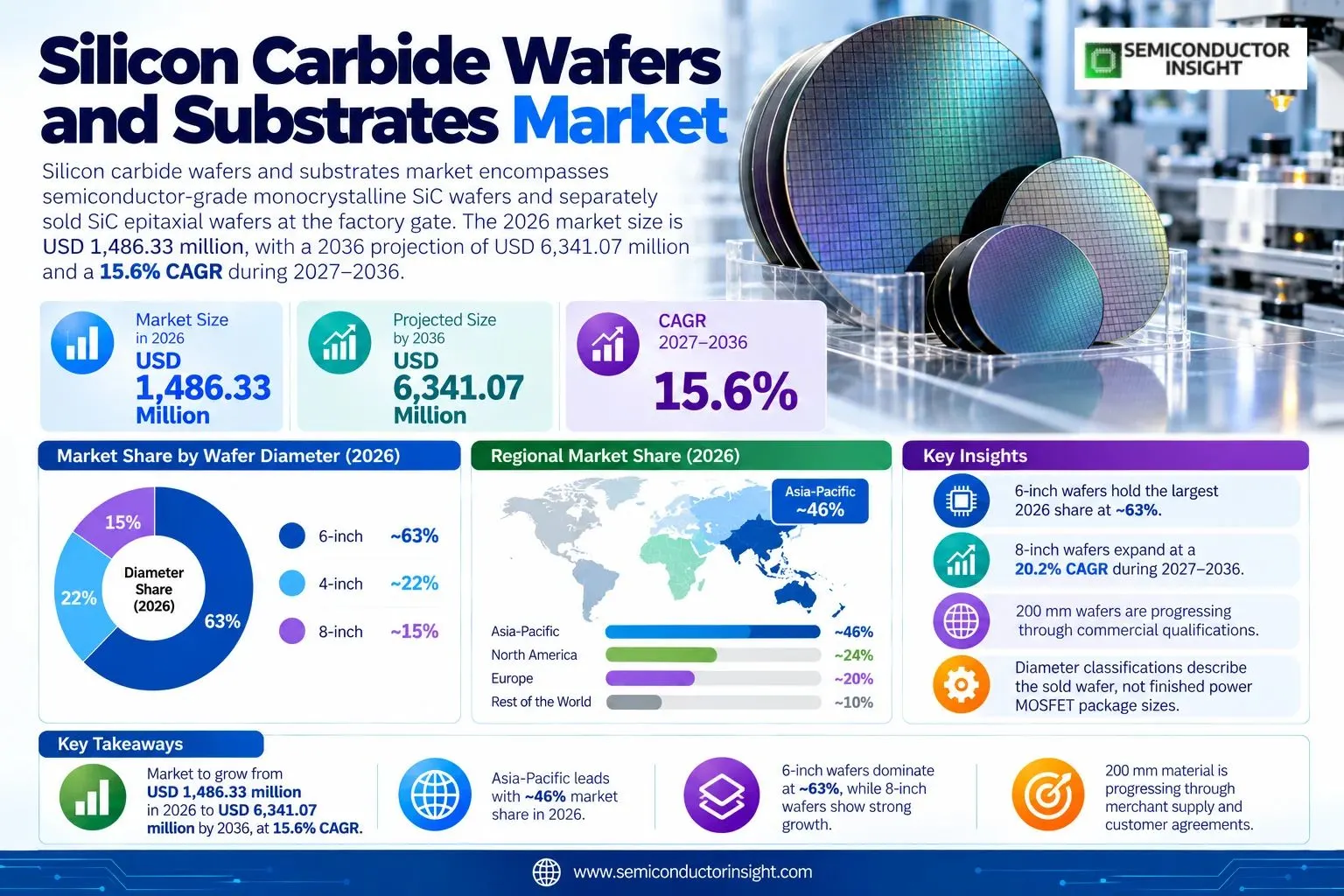
Silicon carbide wafers and substrates market encompasses semiconductor-grade monocrystalline SiC wafers and separately sold SiC epitaxial wafers at the factory gate. The 2026 market size is USD 1,486.33 million, with a 2036 projection of USD 6,341.07 million and a 15.6% CAGR during 2027–2036. Asia-Pacific represents an estimated ~46% of the base-year value, while 150 mm wafers retain the largest diameter category and 200 mm material is progressing through commercial qualifications.

Get the sample PDF with study scope, segmentation and methodology details.

Key Statistics

2026 Market Size
USD 1,486.33 million
2036 Projected Size
USD 6,341.07 million
CAGR (2027–2036)
15.6%
Largest Market in 2026
Asia-Pacific (~46%)

Key Takeaways

  • Market trajectory: silicon carbide wafers and substrates revenue is modeled at USD 1,486.33 million for 2026 and USD 6,341.07 million for 2036, representing 15.6% growth during 2027–2036. The boundary covers merchant single-crystal substrates and externally sold SiC epitaxial wafers, not downstream SiC power transistors or converter assemblies.
  • 150 mm qualification base: 6-inch wafers retain the largest estimated 2026 share at ~63%, supported by established Wolfspeed, SiCrystal, SK Siltron CSS and Asian material qualifications. The 8-inch category is growing faster at ~20.2% CAGR as commercial 200 mm substrate and epi-wafer offerings expand.
  • Power-device end market: Power Devices account for an estimated ~74% of 2026 material revenue because vertical MOSFET and Schottky processes require conductive n-type substrates with controlled defects. Wireless Infrastructure relies on semi-insulating SiC for selected GaN-on-SiC RF devices and is not interchangeable with power-device demand.
  • Regional leadership: Asia-Pacific has an estimated ~46% share of 2026 wafer revenue, supported by Chinese boule and substrate suppliers and Japanese epitaxy capability. North America remains important through Wolfspeed and SK Siltron CSS, while Europe combines SiCrystal supply and engineered-wafer development.
  • Qualification economics: Commercial 200 mm announcements from Wolfspeed and Coherent establish availability of larger wafers, but price and yield depend on micropipe density, dislocations, wafer flatness and epitaxy uniformity. Agreements with Infineon and ST confirm customer sourcing activity without independently auditing global revenue shares or market concentration.

Silicon Carbide Wafers and Substrates Market Overview

Silicon carbide wafers and substrates market encompasses semiconductor-grade monocrystalline SiC wafers and separately sold SiC epitaxial wafers at the factory gate. The 2026 market size is USD 1,486.33 million, with a 2036 projection of USD 6,341.07 million and a 15.6% CAGR during 2027–2036. Asia-Pacific represents an estimated ~46% of the base-year value, while 150 mm wafers retain the largest diameter category and 200 mm material is progressing through commercial qualifications.

Base year: 2026 · Estimate year: 2027 · Forecast year: 2036 · Historical review: 2021–2025 · Values: USD million

The wafer market begins when a semiconductor-grade SiC boule is sliced, ground and polished into a specified substrate suitable for epitaxial growth or direct device processing. Conductive n-type material underpins high-voltage MOSFET and diode manufacturing, while semi-insulating grades support selected GaN-on-SiC RF processes. Revenue from a wafer that moves into an epitaxy facility must not be counted again as an additional bare-wafer sale when the resulting epi-wafer is ultimately invoiced to the device maker.

Wolfspeed introduced commercial 200 mm SiC materials in September 2025 and a premium n-type substrate offering in September 2026. Coherent disclosed shipments of 200 mm substrates and epi-wafers in September 2024, identifying 350-micron and 500-micron wafer options. These dated manufacturer disclosures establish tangible product activity, but the commercial mix across 100 mm, 150 mm and 200 mm wafers remains sensitive to qualification schedules, downstream device yields and the installed equipment base.

Procurement agreements provide another window into demand. Infineon expanded sourcing relationships with SK Siltron CSS, SICC and TanKeBlue for 150 mm material and future diameter transitions, while SiCrystal extended its 150 mm substrate agreement with STMicroelectronics in April 2024. The announced minimum expected value of that SiCrystal arrangement was USD 230 million over several years, not a single-year global market figure. Contract scope and actual shipment timing must be separated when interpreting such announcements.

The production landscape combines merchant specialists and vertically integrated semiconductor manufacturers. SK Siltron CSS disclosed a conditional U.S. financing commitment of up to USD 544 million for its Michigan wafer expansion in February 2024; ST outlined a vertically integrated 200 mm SiC campus in Italy in May 2024. Neither figure represents realized merchant wafer sales. Captive substrates used inside a device producer can influence supply availability without creating a second external substrate transaction.

For the 2027–2036 outlook, 200 mm adoption can increase usable die area per wafer, but the area ratio alone does not determine economic output. Coherent cited a 1.8-fold usable-area benefit relative to 150 mm, whereas defect density, surface flatness, epitaxial uniformity and device-line yield determine the practical conversion. The scenario consequently treats wafer diameter migration as gradual and preserves the distinct economics of power-grade, RF-grade and engineered substrates.

Segment Analysis: By Type

By diameter, the market is segmented into 4-inch, 6-inch and 8-inch SiC wafers. The largest 2026 class is 6-inch at an estimated ~63%, while 8-inch wafers expand at a modeled ~20.2% CAGR. Diameter classifications describe the sold wafer, not finished power MOSFET package sizes. Qualification at 200 mm is progressing through documented merchant supply and customer agreements, but it does not automatically displace existing 150 mm tool capacity.

Wafer diameter Production and buyer characteristics Market position and purchasing implications
4-Inch Wafers Smaller 100 mm wafers remain in selected RF, optoelectronic and older power process flows where installed tools, low-volume qualification and product geometry favour the existing diameter. An estimated ~13% of 2026 substrate revenue remains in this class, and modeled ~10.2% growth is slower than larger formats because major new investment favours 150 mm and 200 mm platforms. In 4-Inch Wafers, at the purchasing stage, technical qualification is separate from capacity reservation: customers check crystal dislocations, wafer bow, surface roughness and the uniformity of epitaxial growth before committing to production lots. Those acceptance criteria explain why a larger nominal diameter does not immediately translate into a lower qualified cost per usable die. Legacy and specialty processes. In 2026 the estimated revenue share is ~13% and the modeled 2026–2036 growth rate is ~10.2% CAGR. Qualified surface finish, micropipe limits, thickness and buyer process windows matter more than the nominal wafer diameter alone; source contracts and qualification lots determine the conversion path. In 4-Inch Wafers, commercial relationships typically involve specification audits, reliability lots, wafer traceability and continuity provisions that extend beyond the quoted unit price. Regional industrial policy can influence the origin of qualified material, yet a new facility does not itself establish external wafer revenue until customers accept its product.
6-Inch Wafers The 150 mm class represents an estimated ~63% of 2026 revenue and retains the broadest documented long-term supply agreements. SiCrystal expanded 150 mm deliveries to ST in 2024, and Infineon has separate 150 mm sourcing relationships with Wolfspeed, SK Siltron CSS, SICC and TanKeBlue. This category supports power-device qualification and established RF processes while larger-wafer transitions proceed. In 6-Inch Wafers, the financial effect appears only when wafer material is transferred to an external buyer; captive internal use is a production indicator rather than an additional merchant sale. Procurement teams also distinguish development samples from qualified repeat orders, because a successful pilot wafer does not guarantee high-volume manufacturing yield. Qualified volume base. In 2026 the estimated revenue share is ~63% and the modeled 2026–2036 growth rate is ~14.4% CAGR. For wafer-diameter selection, Wolfspeed commercialized premium 200 mm n-type substrates in September 2026 with a micropipe specification below 0.01 per square centimeter; that activity illustrates a qualification pathway rather than an audited percentage of merchant substrate sales. In 6-Inch Wafers, conductive n-type material is usually selected for vertical power structures, whereas semi-insulating grades are relevant to RF-on-SiC processes. This distinction changes both the buyer roster and the appropriate yield metric, preventing power-device volume from being treated as equivalent to RF substrate demand.
8-Inch Wafers Commercial 200 mm material is available from Wolfspeed and Coherent, while Infineon expanded its 200 mm wafer supply agreement in October 2026. The estimated ~24% base-year share is smaller than 150 mm, but modeled ~20.2% annual growth reflects capacity conversion and product qualification. Geometry offers more usable area, although low-defect crystal growth and epitaxy uniformity determine realized cost gains. 200 mm conversion opportunity. In 2026 the estimated revenue share is ~24% and the modeled 2026–2036 growth rate is ~20.2% CAGR. Customer decisions involving wafer-diameter selection depend on defect maps and electrical grade; Infineon formalized a 150 mm SiC wafer supply agreement with SICC in May 2023, yet contract announcements do not determine every buyer’s delivered wafer volume. In 8-Inch Wafers, a 200 mm wafer has about 1.78 times the nominal area of a 150 mm wafer, before edge exclusion, process defects and yield losses. The actual number of saleable devices therefore depends on usable area, defect distribution and process capability, not on geometric area alone.

Secondary segmentation: substrate grade and product format

Conductive n-type SiC substrates account for an estimated ~78% of 2026 wafer revenue, while semi-insulating RF-grade substrates hold ~22%. Coherent explicitly offers semi-insulating SiC for GaN-on-SiC RF devices. The conductive share is larger because vertical power-device fabrication uses a broad n-type wafer supply chain; these grades differ in resistivity and device qualification. In grade, commercial relationships typically involve specification audits, reliability lots, wafer traceability and continuity provisions that extend beyond the quoted unit price. The 2026 outlook for wafer-diameter selection distinguishes commercially accepted wafers from capacity promises because Coherent disclosed 200 mm substrate and epitaxial wafer shipments at 350-micron and 500-micron thickness in September 2024; manufacturing evidence alone does not fix selling prices.

Bare polished substrates contribute an estimated ~68% of 2026 merchant revenue and externally sold epitaxial wafers account for ~32%. Coherent shipped both substrates and epi-wafers in 2024, and Wolfspeed offered 200 mm epitaxy for immediate qualification in 2025. The sales boundary follows the final externally invoiced wafer format, preventing double counting of an underlying polished substrate. In format, revenue should be counted at the final externally invoiced material stage: a polished substrate sold to an epitaxy house is one transaction, while an epi-wafer subsequently sold onward is a different product boundary. Combining both without adjustment overstates the final wafer market.

Modeled axis and member Estimated share and growth Revenue scenario allocation
Region: Asia-Pacific 2026 estimated ~46% share; ~15.5% CAGR 2026 modeled value USD 683.7 million; 2036 modeled value USD 2,884.7 million; 46% of base-year material sales.
Region: North America 2026 estimated ~25% share; ~15.2% CAGR 2026 modeled value USD 371.6 million; 2036 modeled value USD 1,529.6 million; 25% of base-year material sales.
Region: Europe 2026 estimated ~22% share; ~15.8% CAGR 2026 modeled value USD 327.0 million; 2036 modeled value USD 1,417.8 million; 22% of base-year material sales.
Region: South America 2026 estimated ~4% share; ~16.9% CAGR 2026 modeled value USD 59.5 million; 2036 modeled value USD 283.3 million; 4% of base-year material sales.
Region: Middle East & Africa 2026 estimated ~3% share; ~17.6% CAGR 2026 modeled value USD 44.6 million; 2036 modeled value USD 225.6 million; 3% of base-year material sales.
Type: 4-Inch Wafers 2026 estimated ~13% share; ~10.2% CAGR 2026 modeled value USD 193.2 million; 2036 modeled value USD 510.4 million; 13% of base-year material sales.
Type: 6-Inch Wafers 2026 estimated ~63% share; ~14.4% CAGR 2026 modeled value USD 936.4 million; 2036 modeled value USD 3,584.9 million; 63% of base-year material sales.
Type: 8-Inch Wafers 2026 estimated ~24% share; ~20.2% CAGR 2026 modeled value USD 356.7 million; 2036 modeled value USD 2,245.8 million; 24% of base-year material sales.
Application: Power Devices 2026 estimated ~74% share; ~16.3% CAGR 2026 modeled value USD 1,099.9 million; 2036 modeled value USD 4,999.5 million; 74% of base-year material sales.
Application: Electronics & Optoelectronics 2026 estimated ~12% share; ~13.3% CAGR 2026 modeled value USD 178.4 million; 2036 modeled value USD 621.7 million; 12% of base-year material sales.
Application: Wireless Infrastructure 2026 estimated ~10% share; ~14.0% CAGR 2026 modeled value USD 148.6 million; 2036 modeled value USD 551.0 million; 10% of base-year material sales.
Application: Others 2026 estimated ~4% share; ~11.0% CAGR 2026 modeled value USD 59.5 million; 2036 modeled value USD 168.8 million; 4% of base-year material sales.
Electrical Grade: Conductive n-Type 2026 estimated ~78% share; ~16.3% CAGR 2026 modeled value USD 1,159.3 million; 2036 modeled value USD 5,231.1 million; 78% of base-year material sales.
Electrical Grade: Semi-Insulating RF Grade 2026 estimated ~22% share; ~13.0% CAGR 2026 modeled value USD 327.0 million; 2036 modeled value USD 1,110.0 million; 22% of base-year material sales.
Product Format: Bare Polished Substrates 2026 estimated ~68% share; ~14.8% CAGR 2026 modeled value USD 1,010.7 million; 2036 modeled value USD 4,035.2 million; 68% of base-year material sales.
Product Format: Epitaxial Wafers 2026 estimated ~32% share; ~17.1% CAGR 2026 modeled value USD 475.6 million; 2036 modeled value USD 2,305.9 million; 32% of base-year material sales.
Buyer Channel: Integrated Device Manufacturers 2026 estimated ~62% share; ~15.8% CAGR 2026 modeled value USD 921.5 million; 2036 modeled value USD 3,993.9 million; 62% of base-year material sales.
Buyer Channel: Independent Power Foundries 2026 estimated ~25% share; ~16.2% CAGR 2026 modeled value USD 371.6 million; 2036 modeled value USD 1,667.7 million; 25% of base-year material sales.
Buyer Channel: RF & Optoelectronic Fabs 2026 estimated ~13% share; ~13.4% CAGR 2026 modeled value USD 193.2 million; 2036 modeled value USD 679.5 million; 13% of base-year material sales.

Segment Analysis: By Application

By application, the original segments are Power Devices, Electronics & Optoelectronics, Wireless Infrastructure and Others. Power Devices hold an estimated ~74% of 2026 revenue because SiC power MOSFET and diode manufacturing uses conductive wafers with stringent defect specifications. Wireless Infrastructure accounts for ~10% through semi-insulating SiC used as a platform for selected RF transistor processes. These are wafer-material applications, not the selling price of downstream electronics.

Application Demand characteristics
Power Devices Power Devices holds an estimated ~74% of 2026 revenue and a modeled ~16.3% CAGR through 2036. Automotive traction inverters, industrial drives, energy storage and high-voltage charging motivate substrate qualification, while Wolfspeed and Infineon have expanded the supply of conductive n-type material. Buyers check crystal defectivity and epitaxial thickness consistency before moving to production. In Power Devices, at the purchasing stage, technical qualification is separate from capacity reservation: customers check crystal dislocations, wafer bow, surface roughness and the uniformity of epitaxial growth before committing to production lots. A supplier targeting power and RF applications must satisfy crystal quality and surface specifications before volume orders; Soitec reported validation of 150 mm SmartSiC substrates with Diodes in November 2025, making product qualification more informative than factory investment alone.
Electronics & Optoelectronics Electronics & Optoelectronics holds an estimated ~12% of 2026 revenue and a modeled ~13.3% CAGR through 2036. Selected optical and electronic structures use specialized SiC wafer properties, but this category is smaller than the high-volume power channel. Device architecture and crystal grade determine suitability, and thermal-only AI packaging material remains outside the semiconductor-grade boundary. In Electronics & Optoelectronics, the financial effect appears only when wafer material is transferred to an external buyer; captive internal use is a production indicator rather than an additional merchant sale. In power and RF applications, a 150 mm to 200 mm transition requires both wafer consistency and customer process changes; SiCrystal expanded its German 150 mm substrate supply agreement with ST in April 2024, while the final revenue event remains an external invoice.
Wireless Infrastructure Wireless Infrastructure holds an estimated ~10% of 2026 revenue and a modeled ~14.0% CAGR through 2036. Semi-insulating SiC can host GaN RF epitaxy for base-station and microwave power amplifiers, as Coherent describes in its RF materials catalogue. This material is included as a wafer input, whereas complete RF amplifiers and radio equipment revenue are excluded. In Wireless Infrastructure, for high-voltage power semiconductors, defect density and resistivity determine downstream electrical yield as much as nominal wafer diameter. Consequently, customers may retain a qualified 150 mm process while separately validating 200 mm lines, and purchase agreements can span both diameters during the conversion period.
Others Others holds an estimated ~4% of 2026 revenue and a modeled ~11.0% CAGR through 2036. Research-to-production qualification, specialty semiconductor structures and low-volume industrial buyers are grouped here only when the externally sold product is a qualifying SiC substrate or epi-wafer. Powder, ceramics and device-level transactions are excluded. In Others, commercial relationships typically involve specification audits, reliability lots, wafer traceability and continuity provisions that extend beyond the quoted unit price. The power and RF applications purchasing channel evaluates traceability and lot-to-lot yield rather than wafer diameter in isolation; Infineon started rolling out power devices fabricated on 200 mm SiC wafers in February 2025, providing a concrete industrial example.

Application demand is not interchangeable with finished device revenue. A power semiconductor maker may buy conductive 150 mm wafers and fabricate multiple device families from the same substrate specification, whereas an RF foundry may need semi-insulating material and a different epitaxy process. Consequently, a procurement agreement for 200 mm power wafers is evidence of substrate qualification, not evidence that every GaN-on-SiC RF wafer or downstream module shares the same sales cycle.

The application mix also affects forecasting. Automotive and industrial customers impose long reliability and traceability cycles, making an announced capacity expansion a leading indicator rather than immediate shipment revenue. Specialty optical and wireless applications can carry higher technical specifications but smaller wafer volumes. This separation is important when interpreting 2026–2036 modeled shares and comparing material revenue with the much larger value of complete inverters or RF systems.
Regional Analysis

Five global regions are compared on estimated 2026 wafer revenue and differentiated growth rates. Asia-Pacific leads with ~46% because of Chinese substrate suppliers and Japanese epitaxy capability; North America follows at ~25% through Wolfspeed and SK Siltron CSS, and Europe accounts for ~22% through SiCrystal, Soitec and integrated device-maker demand. South America and Middle East & Africa are smaller, primarily import-linked demand locations rather than documented large-scale merchant crystal production hubs.

Which regions lead SiC wafer production and qualified material demand?

Regional concentration reflects where semiconductor-grade SiC boules are grown, polished wafers are qualified and epi-wafers are externally sold, rather than where a final electric vehicle or inverter is assembled. A long-term wafer contract between a U.S. supplier and a European device manufacturer can involve multiple geographic stages. The model assigns each merchant wafer transaction to the relevant regional revenue boundary once and treats downstream application demand as a separate indicator.

Region Position Growth outlook Demand profile What decides supplier selection
Asia-Pacific Largest (~46%) ~15.5% CAGR China Crystal quality, qualification and Chinese suppliers SICC and TanKeBlue have direct Infineon wafer contracts;
North America Second (~25%) ~15.2% CAGR United States Crystal quality, qualification and Wolfspeed sells 200 mm n-type substrates and epi-wafers, while SK Siltron C
Europe Third (~22%) ~15.8% CAGR Germany Crystal quality, qualification and SiCrystal manufactures 150 mm substrates in Germany, Soitec develops engine
South America Emerging (~4%) ~16.9% CAGR Brazil Crystal quality, qualification and The region primarily consumes imported power electronics and industrial sys
Middle East & Africa Emerging (~3%) ~17.6% CAGR Israel Crystal quality, qualification and This region has research, energy-transition and high-reliability electronic

Asia-Pacific LARGEST · ~46% SHARE

What determines semiconductor-grade SiC wafer demand in Asia-Pacific?

Asia-Pacific represents an estimated ~46% of 2026 global merchant SiC wafer revenue and a modeled ~15.5% CAGR through 2036. Chinese suppliers SICC and TanKeBlue have direct Infineon wafer contracts; Japan-based Resonac supplies SiC materials and epitaxy, while ST and other device firms maintain Asian power fabs. The regional position is a wafer-material estimate, not a tally of complete power-device or converter sales. Customer qualification of 150 mm and 200 mm materials determines whether announced supply and capacity translates into accepted shipments.

Market positionLargest (~46% share)
Growth outlookModeled ~15.5% CAGR
Demand profilePower-grade and RF-grade wafers
Market access gateSupplier qualification and wafer traceability
Country Position in region What drives demand
China Major supply SICC and TanKeBlue have 150 mm wafer agreements with Infineon, and both agreements identify future 200 mm transition work. Their inclusion is based on documented merchant sourcing, not an assumption that every Chinese SiC materials enterprise ships qualified device-grade wafers. In China, for high-voltage power semiconductors, defect density and resistivity determine downstream electrical yield as much as nominal wafer diameter. For material sold into Asia-Pacific, conductive and semi-insulating specifications have different acceptance criteria; Soitec and Tokai Carbon agreed in May 2024 to develop poly-SiC handle material for engineered SmartSiC wafers, which must be interpreted within the appropriate product boundary.
Japan Qualification channel Resonac disclosed SiC epitaxial wafer development and a 2025 GSC award; its Infineon supply relationship spans 150 mm materials with a path toward 200 mm. Japan therefore participates through high-value crystal and epitaxy processes as well as downstream power-device customers. In Japan, commercial relationships typically involve specification audits, reliability lots, wafer traceability and continuity provisions that extend beyond the quoted unit price. The economic importance of Asia-Pacific lies in reliable deliveries after inspection and epitaxy acceptance; Infineon and Wolfspeed extended their wafer supply relationship to 200 mm substrates in October 2026, without independently verifying the global substrate-market denominator.
South Korea and Taiwan End-use linkage SK Siltron CSS combines Korean ownership with U.S. SiC wafer manufacturing, while Taiwan has power-device and RF semiconductor processing capabilities. Regional demand depends on qualification and external wafer procurement rather than the nominal headquarters of an integrated device maker. In South Korea and Taiwan, conductive n-type material is usually selected for vertical power structures, whereas semi-insulating grades are relevant to RF-on-SiC processes. The Asia-Pacific revenue scenario excludes finished transistors and internal transfer values; TanKeBlue agreed to supply 150 mm SiC wafers and boules to Infineon in May 2023, so announced investment or device sales cannot be added to merchant wafer receipts.

Market instances

  • Asia-Pacific wafer sourcing and diameter conversion. Procurement for Asia-Pacific separates development samples from repeat shipments; SK Siltron CSS announced conditional financing for a Michigan SiC wafer capacity expansion in February 2024, underscoring why technical availability and recurring wafer revenue are different measures. For this region the estimated 2026 share is ~46% and the 2036 model uses ~15.5% annual growth. The key transaction is the externally sold wafer or epi-wafer, not a finished semiconductor or a fabrication plant investment. Regional trade and qualification relationships can therefore cross borders before the wafer reaches the customer.
  • Asia-Pacific buyer qualification and grade selection. Commercial participation around Asia-Pacific can span crystal growth, polished substrates and epitaxy; ST outlined a vertically integrated 200 mm SiC manufacturing campus in Italy in May 2024, but the final wafer is counted once when invoiced to an external buyer. Across Asia-Pacific, defect density and wafer shape govern usable device area; Resonac received a 2025 industrial chemistry award for its SiC epitaxial wafer technology, with customer acceptance remaining a stronger signal than nominal factory capacity. Supplier selection distinguishes conductive n-type material for power devices from semi-insulating SiC for RF, with different wafer resistivity and epitaxial requirements. The model preserves this distinction while assigning revenue to the external substrate invoice rather than to device assembly.
  • Asia-Pacific manufacturing and demand boundary. For Asia-Pacific, Infineon and Wolfspeed extended their wafer supply relationship to 200 mm substrates in October 2026; that activity illustrates a qualification pathway rather than an audited percentage of merchant substrate sales. Customer decisions involving Asia-Pacific depend on defect maps and electrical grade; TanKeBlue agreed to supply 150 mm SiC wafers and boules to Infineon in May 2023, yet contract announcements do not determine every buyer’s delivered wafer volume. New capacity and development agreements matter because they change available wafer formats, but a 2026 market allocation must not treat planned facilities as completed shipments. Acceptance testing, repeat lot quality and pricing establish the revenue path through 2036.
In the full report: detailed Asia-Pacific wafer revenue, material grade, 100 mm/150 mm/200 mm qualification, country-level shipments, merchant versus captive sourcing and customer supply agreements.

North America SECOND LARGEST · ~25% SHARE

What determines semiconductor-grade SiC wafer demand in North America?

North America represents an estimated ~25% of 2026 global merchant SiC wafer revenue and a modeled ~15.2% CAGR through 2036. Wolfspeed sells 200 mm n-type substrates and epi-wafers, while SK Siltron CSS is expanding its Michigan production. The regional position reflects both domestic wafer production and long-term supply to power-device customers. The 2026 outlook for North America distinguishes commercially accepted wafers from capacity promises because SK Siltron CSS announced conditional financing for a Michigan SiC wafer capacity expansion in February 2024; manufacturing evidence alone does not fix selling prices. A supplier targeting North America must satisfy crystal quality and surface specifications before volume orders; ST outlined a vertically integrated 200 mm SiC manufacturing campus in Italy in May 2024, making product qualification more informative than factory investment alone.

Market positionSecond largest (~25% share)
Growth outlookModeled ~15.2% CAGR
Demand profilePower-grade and RF-grade wafers
Market access gateSupplier qualification and wafer traceability
Country Position in region What drives demand
United States Major supply Wolfspeed announced commercial 200 mm materials in 2025 and premium 200 mm n-type substrates in 2026. SK Siltron CSS disclosed a conditional USD 544 million financing commitment for its Michigan SiC wafer expansion in 2024; financing is capacity support rather than wafer revenue. In United States, commercial relationships typically involve specification audits, reliability lots, wafer traceability and continuity provisions that extend beyond the quoted unit price. In North America, a 150 mm to 200 mm transition requires both wafer consistency and customer process changes; Resonac received a 2025 industrial chemistry award for its SiC epitaxial wafer technology, while the final revenue event remains an external invoice.
Canada Qualification channel Canadian buyers participate principally through semiconductor research, industrial power-electronics design and cross-border supply chains rather than a large publicly documented merchant SiC boule base. Qualification may occur locally while volume wafer production and invoicing remain concentrated in the United States. In Canada, conductive n-type material is usually selected for vertical power structures, whereas semi-insulating grades are relevant to RF-on-SiC processes. The North America purchasing channel evaluates traceability and lot-to-lot yield rather than wafer diameter in isolation; Wolfspeed commercialized premium 200 mm n-type substrates in September 2026 with a micropipe specification below 0.01 per square centimeter, providing a concrete industrial example.
Mexico End-use linkage Mexican automotive and industrial electronics assembly creates indirect demand for SiC power devices, but the wafer market counts substrate transactions at the material supplier stage. End-use vehicle or converter revenue in Mexico must not be mistaken for merchant SiC wafer sales originating in that country. In Mexico, a 200 mm wafer has about 1.78 times the nominal area of a 150 mm wafer, before edge exclusion, process defects and yield losses. For material sold into North America, conductive and semi-insulating specifications have different acceptance criteria; Infineon formalized a 150 mm SiC wafer supply agreement with SICC in May 2023, which must be interpreted within the appropriate product boundary.

Market instances

  • North America wafer sourcing and diameter conversion. The economic importance of North America lies in reliable deliveries after inspection and epitaxy acceptance; Coherent disclosed 200 mm substrate and epitaxial wafer shipments at 350-micron and 500-micron thickness in September 2024, without independently verifying the global substrate-market denominator. The North America revenue scenario excludes finished transistors and internal transfer values; Soitec reported validation of 150 mm SmartSiC substrates with Diodes in November 2025, so announced investment or device sales cannot be added to merchant wafer receipts. For this region the estimated 2026 share is ~25% and the 2036 model uses ~15.2% annual growth. Procurement for North America separates development samples from repeat shipments; SiCrystal expanded its German 150 mm substrate supply agreement with ST in April 2024, underscoring why technical availability and recurring wafer revenue are different measures. Commercial participation around North America can span crystal growth, polished substrates and epitaxy; Infineon started rolling out power devices fabricated on 200 mm SiC wafers in February 2025, but the final wafer is counted once when invoiced to an external buyer.
  • North America buyer qualification and grade selection. Across North America, defect density and wafer shape govern usable device area; Soitec and Tokai Carbon agreed in May 2024 to develop poly-SiC handle material for engineered SmartSiC wafers, with customer acceptance remaining a stronger signal than nominal factory capacity. For North America, Coherent disclosed 200 mm substrate and epitaxial wafer shipments at 350-micron and 500-micron thickness in September 2024; that activity illustrates a qualification pathway rather than an audited percentage of merchant substrate sales. Customer decisions involving North America depend on defect maps and electrical grade; Soitec reported validation of 150 mm SmartSiC substrates with Diodes in November 2025, yet contract announcements do not determine every buyer’s delivered wafer volume. The 2026 outlook for North America distinguishes commercially accepted wafers from capacity promises because SiCrystal expanded its German 150 mm substrate supply agreement with ST in April 2024; manufacturing evidence alone does not fix selling prices.
  • North America manufacturing and demand boundary. A supplier targeting North America must satisfy crystal quality and surface specifications before volume orders; Infineon started rolling out power devices fabricated on 200 mm SiC wafers in February 2025, making product qualification more informative than factory investment alone. In North America, a 150 mm to 200 mm transition requires both wafer consistency and customer process changes; Soitec and Tokai Carbon agreed in May 2024 to develop poly-SiC handle material for engineered SmartSiC wafers, while the final revenue event remains an external invoice. The North America purchasing channel evaluates traceability and lot-to-lot yield rather than wafer diameter in isolation; Infineon and Wolfspeed extended their wafer supply relationship to 200 mm substrates in October 2026, providing a concrete industrial example. For material sold into North America, conductive and semi-insulating specifications have different acceptance criteria; TanKeBlue agreed to supply 150 mm SiC wafers and boules to Infineon in May 2023, which must be interpreted within the appropriate product boundary.
In the full report: detailed North America wafer revenue, material grade, 100 mm/150 mm/200 mm qualification, country-level shipments, merchant versus captive sourcing and customer supply agreements.

Europe THIRD LARGEST · ~22% SHARE

What determines semiconductor-grade SiC wafer demand in Europe?

Europe represents an estimated ~22% of 2026 global merchant SiC wafer revenue and a modeled ~15.8% CAGR through 2036. SiCrystal manufactures 150 mm substrates in Germany, Soitec develops engineered SmartSiC material in France, and ST is building integrated SiC capacity in Italy. European customers increasingly seek dual-sourced wafers. The economic importance of Europe lies in reliable deliveries after inspection and epitaxy acceptance; SK Siltron CSS announced conditional financing for a Michigan SiC wafer capacity expansion in February 2024, without independently verifying the global substrate-market denominator. The Europe revenue scenario excludes finished transistors and internal transfer values; ST outlined a vertically integrated 200 mm SiC manufacturing campus in Italy in May 2024, so announced investment or device sales cannot be added to merchant wafer receipts.

Market positionThird largest (~22% share)
Growth outlookModeled ~15.8% CAGR
Demand profilePower-grade and RF-grade wafers
Market access gateSupplier qualification and wafer traceability
Country Position in region What drives demand
Germany Major supply SiCrystal, part of ROHM, expanded its 150 mm substrate wafer agreement with ST in April 2024, with a minimum expected multiyear value of USD 230 million. Germany also hosts major power semiconductor customers that qualify wafers for automotive and industrial use. In Germany, conductive n-type material is usually selected for vertical power structures, whereas semi-insulating grades are relevant to RF-on-SiC processes. Procurement for Europe separates development samples from repeat shipments; Resonac received a 2025 industrial chemistry award for its SiC epitaxial wafer technology, underscoring why technical availability and recurring wafer revenue are different measures.
France Qualification channel Soitec and Tokai Carbon agreed in May 2024 on poly-SiC handle wafer supply for SmartSiC engineered substrates, and Soitec later disclosed Diodes validation of 150 mm SmartSiC for power-device processing. Handle-wafer inputs are not separately counted as finished merchant single-crystal substrates. In France, a 200 mm wafer has about 1.78 times the nominal area of a 150 mm wafer, before edge exclusion, process defects and yield losses. Commercial participation around Europe can span crystal growth, polished substrates and epitaxy; Wolfspeed commercialized premium 200 mm n-type substrates in September 2026 with a micropipe specification below 0.01 per square centimeter, but the final wafer is counted once when invoiced to an external buyer.
Italy and Austria End-use linkage ST outlined a 200 mm vertically integrated campus in Catania in May 2024, while Infineon started delivering 200 mm SiC device products from Villach in early 2025. These announcements signal European processing demand but include captive operations that do not automatically enter merchant substrate sales. In Italy and Austria, revenue should be counted at the final externally invoiced material stage: a polished substrate sold to an epitaxy house is one transaction, while an epi-wafer subsequently sold onward is a different product boundary. Combining both without adjustment overstates the final wafer market.

Market instances

  • Europe wafer sourcing and diameter conversion. Across Europe, defect density and wafer shape govern usable device area; Infineon formalized a 150 mm SiC wafer supply agreement with SICC in May 2023, with customer acceptance remaining a stronger signal than nominal factory capacity. European customers increasingly seek dual-sourced wafers. For this region the estimated 2026 share is ~22% and the 2036 model uses ~15.8% annual growth. For Europe, SK Siltron CSS announced conditional financing for a Michigan SiC wafer capacity expansion in February 2024; that activity illustrates a qualification pathway rather than an audited percentage of merchant substrate sales. Customer decisions involving Europe depend on defect maps and electrical grade; ST outlined a vertically integrated 200 mm SiC manufacturing campus in Italy in May 2024, yet contract announcements do not determine every buyer’s delivered wafer volume.
  • Europe buyer qualification and grade selection. The 2026 outlook for Europe distinguishes commercially accepted wafers from capacity promises because Resonac received a 2025 industrial chemistry award for its SiC epitaxial wafer technology; manufacturing evidence alone does not fix selling prices. A supplier targeting Europe must satisfy crystal quality and surface specifications before volume orders; Wolfspeed commercialized premium 200 mm n-type substrates in September 2026 with a micropipe specification below 0.01 per square centimeter, making product qualification more informative than factory investment alone. In Europe, a 150 mm to 200 mm transition requires both wafer consistency and customer process changes; Infineon formalized a 150 mm SiC wafer supply agreement with SICC in May 2023, while the final revenue event remains an external invoice. The Europe purchasing channel evaluates traceability and lot-to-lot yield rather than wafer diameter in isolation; Coherent disclosed 200 mm substrate and epitaxial wafer shipments at 350-micron and 500-micron thickness in September 2024, providing a concrete industrial example.
  • Europe manufacturing and demand boundary. For material sold into Europe, conductive and semi-insulating specifications have different acceptance criteria; Soitec reported validation of 150 mm SmartSiC substrates with Diodes in November 2025, which must be interpreted within the appropriate product boundary. Handle-wafer inputs are not separately counted as finished merchant single-crystal substrates. The economic importance of Europe lies in reliable deliveries after inspection and epitaxy acceptance; SiCrystal expanded its German 150 mm substrate supply agreement with ST in April 2024, without independently verifying the global substrate-market denominator. The Europe revenue scenario excludes finished transistors and internal transfer values; Infineon started rolling out power devices fabricated on 200 mm SiC wafers in February 2025, so announced investment or device sales cannot be added to merchant wafer receipts.
In the full report: detailed Europe wafer revenue, material grade, 100 mm/150 mm/200 mm qualification, country-level shipments, merchant versus captive sourcing and customer supply agreements.

South America DEVELOPING · ~4% SHARE

What determines semiconductor-grade SiC wafer demand in South America?

South America represents an estimated ~4% of 2026 global merchant SiC wafer revenue and a modeled ~16.9% CAGR through 2036. The region primarily consumes imported power electronics and industrial systems, while documented commercial SiC crystal growth capacity is limited compared with Asia, North America and Europe. Estimated wafer revenue is correspondingly small. Procurement for South America separates development samples from repeat shipments; Soitec and Tokai Carbon agreed in May 2024 to develop poly-SiC handle material for engineered SmartSiC wafers, underscoring why technical availability and recurring wafer revenue are different measures. Commercial participation around South America can span crystal growth, polished substrates and epitaxy; Infineon and Wolfspeed extended their wafer supply relationship to 200 mm substrates in October 2026, but the final wafer is counted once when invoiced to an external buyer.

Market positionDeveloping (~4% share)
Growth outlookModeled ~16.9% CAGR
Demand profileSpecialty procurement
Market access gateExternal merchant wafer orders
Country Position in region What drives demand
Brazil Specialty demand Solar inverters, industrial motors and charging equipment can contain SiC power devices, yet their finished equipment value is not the wafer market. Direct wafer demand arises only where semiconductor research, assembly-linked process development or specialty fabrication purchases qualifying SiC material. In Brazil, a 200 mm wafer has about 1.78 times the nominal area of a 150 mm wafer, before edge exclusion, process defects and yield losses. Across South America, defect density and wafer shape govern usable device area; TanKeBlue agreed to supply 150 mm SiC wafers and boules to Infineon in May 2023, with customer acceptance remaining a stronger signal than nominal factory capacity.
Argentina Qualification channel Industrial power infrastructure and academic materials research can create small specialty-wafer orders, but the existence of electric-power projects does not prove local semiconductor-grade substrate manufacturing. The modeled share is therefore modest and should be read as an analytical allocation. In Argentina, revenue should be counted at the final externally invoiced material stage: a polished substrate sold to an epitaxy house is one transaction, while an epi-wafer subsequently sold onward is a different product boundary. Combining both without adjustment overstates the final wafer market.
Chile End-use linkage Mining electrification and renewable-energy projects create downstream demand for high-efficiency conversion, which may stimulate imported SiC device adoption. The merchant substrate transaction generally occurs earlier in the supply chain outside Chile, preventing local equipment spending from being assigned to wafer sales. In Chile, suppliers that can deliver consistent thickness, doping and low micropipe density gain an advantage in long qualification cycles. Those engineering factors can outweigh a short-term wafer price concession when the downstream MOSFET process carries high capital and failure costs.

Market instances

  • South America wafer sourcing and diameter conversion. For South America, SiCrystal expanded its German 150 mm substrate supply agreement with ST in April 2024; that activity illustrates a qualification pathway rather than an audited percentage of merchant substrate sales. Estimated wafer revenue is correspondingly small. For this region the estimated 2026 share is ~4% and the 2036 model uses ~16.9% annual growth. Customer decisions involving South America depend on defect maps and electrical grade; Infineon started rolling out power devices fabricated on 200 mm SiC wafers in February 2025, yet contract announcements do not determine every buyer’s delivered wafer volume. The 2026 outlook for South America distinguishes commercially accepted wafers from capacity promises because Soitec and Tokai Carbon agreed in May 2024 to develop poly-SiC handle material for engineered SmartSiC wafers; manufacturing evidence alone does not fix selling prices.
  • South America buyer qualification and grade selection. A supplier targeting South America must satisfy crystal quality and surface specifications before volume orders; Infineon and Wolfspeed extended their wafer supply relationship to 200 mm substrates in October 2026, making product qualification more informative than factory investment alone. In South America, a 150 mm to 200 mm transition requires both wafer consistency and customer process changes; TanKeBlue agreed to supply 150 mm SiC wafers and boules to Infineon in May 2023, while the final revenue event remains an external invoice. The South America purchasing channel evaluates traceability and lot-to-lot yield rather than wafer diameter in isolation; SK Siltron CSS announced conditional financing for a Michigan SiC wafer capacity expansion in February 2024, providing a concrete industrial example. For material sold into South America, conductive and semi-insulating specifications have different acceptance criteria; ST outlined a vertically integrated 200 mm SiC manufacturing campus in Italy in May 2024, which must be interpreted within the appropriate product boundary.
  • South America manufacturing and demand boundary. The economic importance of South America lies in reliable deliveries after inspection and epitaxy acceptance; Resonac received a 2025 industrial chemistry award for its SiC epitaxial wafer technology, without independently verifying the global substrate-market denominator. The South America revenue scenario excludes finished transistors and internal transfer values; Wolfspeed commercialized premium 200 mm n-type substrates in September 2026 with a micropipe specification below 0.01 per square centimeter, so announced investment or device sales cannot be added to merchant wafer receipts. Procurement for South America separates development samples from repeat shipments; Infineon formalized a 150 mm SiC wafer supply agreement with SICC in May 2023, underscoring why technical availability and recurring wafer revenue are different measures. Commercial participation around South America can span crystal growth, polished substrates and epitaxy; Coherent disclosed 200 mm substrate and epitaxial wafer shipments at 350-micron and 500-micron thickness in September 2024, but the final wafer is counted once when invoiced to an external buyer.
In the full report: detailed South America wafer revenue, material grade, 100 mm/150 mm/200 mm qualification, country-level shipments, merchant versus captive sourcing and customer supply agreements.

Middle East & Africa EMERGING · ~3% SHARE

What determines semiconductor-grade SiC wafer demand in Middle East & Africa?

Middle East & Africa represents an estimated ~3% of 2026 global merchant SiC wafer revenue and a modeled ~17.6% CAGR through 2036. This region has research, energy-transition and high-reliability electronics opportunities but limited publicly documented high-volume merchant SiC crystal manufacturing. Demand is concentrated in specialty procurement and imported device supply chains. Across Middle East & Africa, defect density and wafer shape govern usable device area; Soitec reported validation of 150 mm SmartSiC substrates with Diodes in November 2025, with customer acceptance remaining a stronger signal than nominal factory capacity. For Middle East & Africa, Resonac received a 2025 industrial chemistry award for its SiC epitaxial wafer technology; that activity illustrates a qualification pathway rather than an audited percentage of merchant substrate sales.

Market positionEmerging (~3% share)
Growth outlookModeled ~17.6% CAGR
Demand profileSpecialty procurement
Market access gateExternal merchant wafer orders
Country Position in region What drives demand
Israel Specialty demand Advanced electronics design and research activities can require specialty SiC substrates for RF or power prototyping. Qualification lots are relevant to the material market only when the wafer is externally purchased; laboratory funding and finished semiconductor revenue remain separate categories. In Israel, revenue should be counted at the final externally invoiced material stage: a polished substrate sold to an epitaxy house is one transaction, while an epi-wafer subsequently sold onward is a different product boundary. Combining both without adjustment overstates the final wafer market.
United Arab Emirates and Saudi Arabia Qualification channel Data-centre power infrastructure, solar projects and industrial electrification can increase downstream interest in SiC devices. These end uses support a longer-term wafer demand pathway, although the actual wafer invoice is usually issued by an overseas materials supplier. In United Arab Emirates and Saudi Arabia, suppliers that can deliver consistent thickness, doping and low micropipe density gain an advantage in long qualification cycles. Customer decisions involving Middle East & Africa depend on defect maps and electrical grade; Wolfspeed commercialized premium 200 mm n-type substrates in September 2026 with a micropipe specification below 0.01 per square centimeter, yet contract announcements do not determine every buyer’s delivered wafer volume.
South Africa End-use linkage Industrial drives, renewable-power integration and scientific laboratories may purchase semiconductor materials or use imported SiC-based converters. The modeled regional allocation stays limited because end-market adoption is not evidence of a broad domestic merchant wafer-production ecosystem. In South Africa, contract announcements signal buyer qualification and planned capacity, but contract face values and government financing do not directly equal annual semiconductor-grade wafer sales. A revenue model must separate executed deliveries from investment commitments and potential future production.

Market instances

  • Middle East & Africa wafer sourcing and diameter conversion. The 2026 outlook for Middle East & Africa distinguishes commercially accepted wafers from capacity promises because Infineon formalized a 150 mm SiC wafer supply agreement with SICC in May 2023; manufacturing evidence alone does not fix selling prices. Demand is concentrated in specialty procurement and imported device supply chains. For this region the estimated 2026 share is ~3% and the 2036 model uses ~17.6% annual growth. A supplier targeting Middle East & Africa must satisfy crystal quality and surface specifications before volume orders; Coherent disclosed 200 mm substrate and epitaxial wafer shipments at 350-micron and 500-micron thickness in September 2024, making product qualification more informative than factory investment alone. In Middle East & Africa, a 150 mm to 200 mm transition requires both wafer consistency and customer process changes; Soitec reported validation of 150 mm SmartSiC substrates with Diodes in November 2025, while the final revenue event remains an external invoice.
  • Middle East & Africa buyer qualification and grade selection. The Middle East & Africa purchasing channel evaluates traceability and lot-to-lot yield rather than wafer diameter in isolation; SiCrystal expanded its German 150 mm substrate supply agreement with ST in April 2024, providing a concrete industrial example. For material sold into Middle East & Africa, conductive and semi-insulating specifications have different acceptance criteria; Infineon started rolling out power devices fabricated on 200 mm SiC wafers in February 2025, which must be interpreted within the appropriate product boundary. The economic importance of Middle East & Africa lies in reliable deliveries after inspection and epitaxy acceptance; Soitec and Tokai Carbon agreed in May 2024 to develop poly-SiC handle material for engineered SmartSiC wafers, without independently verifying the global substrate-market denominator. The Middle East & Africa revenue scenario excludes finished transistors and internal transfer values; Infineon and Wolfspeed extended their wafer supply relationship to 200 mm substrates in October 2026, so announced investment or device sales cannot be added to merchant wafer receipts.
  • Middle East & Africa manufacturing and demand boundary. Procurement for Middle East & Africa separates development samples from repeat shipments; TanKeBlue agreed to supply 150 mm SiC wafers and boules to Infineon in May 2023, underscoring why technical availability and recurring wafer revenue are different measures. Commercial participation around Middle East & Africa can span crystal growth, polished substrates and epitaxy; SK Siltron CSS announced conditional financing for a Michigan SiC wafer capacity expansion in February 2024, but the final wafer is counted once when invoiced to an external buyer. Across Middle East & Africa, defect density and wafer shape govern usable device area; ST outlined a vertically integrated 200 mm SiC manufacturing campus in Italy in May 2024, with customer acceptance remaining a stronger signal than nominal factory capacity. For Middle East & Africa, Soitec and Tokai Carbon agreed in May 2024 to develop poly-SiC handle material for engineered SmartSiC wafers; that activity illustrates a qualification pathway rather than an audited percentage of merchant substrate sales.
In the full report: detailed Middle East & Africa wafer revenue, material grade, 100 mm/150 mm/200 mm qualification, country-level shipments, merchant versus captive sourcing and customer supply agreements.

Key Silicon Carbide Wafer Manufacturers and Competitive Landscape

Competition is driven by low-defect bulk crystal growth, polishing and epitaxial control rather than the number of downstream SiC devices sold. Wolfspeed and Coherent have documented commercial 200 mm materials, SiCrystal and SK Siltron CSS hold multiyear substrate supply relationships, and Resonac contributes epitaxial material expertise. Soitec engineered SmartSiC substrates form a distinct technology path that must not be confused with bulk single-crystal wafer output.

Wolfspeed has a broad commercial SiC materials offering and announced premium 200 mm n-type substrates in September 2026. Its October 2026 expanded Infineon supply agreement establishes an external customer relationship across the 150 mm to 200 mm transition. The relevant competitive strengths are defect control, manufacturing consistency and customer process compatibility; the announcements do not provide a verified global wafer market-share ranking.

Coherent disclosed shipment of 200 mm substrates and epitaxial wafers in September 2024, covering 350-micron and 500-micron thickness options. The company also offers semi-insulating SiC grades for GaN-on-SiC RF electronics. These are materially different buyer specifications: a vertical power device values conductive substrate quality, whereas RF fabs prioritize high resistivity and suitable crystal polytype. Both belong to the semiconductor-grade wafer supply chain, not to finished device revenue.

SiCrystal, the ROHM group wafer supplier, expanded its 150 mm substrate agreement with STMicroelectronics in April 2024. SK Siltron CSS secured an Infineon sourcing agreement and described a U.S. wafer capacity expansion, while Infineon separately contracted SICC and TanKeBlue for SiC material. These agreements identify direct-fit supplier relationships; company names without verified external wafer offerings should not be ranked as merchant wafer sellers.

Resonac and Soitec are active in advanced SiC material development and epitaxy, including a 2024 agreement on 200 mm bonded substrates. Soitec disclosed 150 mm SmartSiC validation with Diodes in November 2025. A bonded engineered wafer differs structurally from a monocrystalline bulk substrate, so a competitive comparison must specify product type and qualification status rather than aggregating every announced wafer platform into identical merchant sales.

Tier structure

Tier Companies Basis of competition
Established merchant substrate suppliers Wolfspeed; Coherent; SiCrystal (ROHM); SK Siltron CSS; SICC; TanKeBlue These companies have direct product disclosures or identified customer supply agreements for SiC substrate wafers. Competitive position depends on repeatability of low-defect material, qualification in customer power or RF processes and the ability to deliver 150 mm or 200 mm lots consistently. The grouping is evidence of commercial participation rather than an audited revenue ranking. In tier-one, for high-voltage power semiconductors, defect density and resistivity determine downstream electrical yield as much as nominal wafer diameter. Customer decisions involving supplier competition depend on defect maps and electrical grade; Infineon and Wolfspeed extended their wafer supply relationship to 200 mm substrates in October 2026, yet contract announcements do not determine every buyer’s delivered wafer volume.
Epitaxy and engineered substrate specialists Resonac; Soitec; Coherent; Wolfspeed Resonac is linked to SiC epitaxial materials and 200 mm bonded-wafer development, while Soitec supplies engineered SmartSiC structures that differ from bulk monocrystalline substrates. Coherent and Wolfspeed also offer epi-wafer products. Product stage must be explicit when comparing these businesses to avoid adding substrate input revenue twice. In tier-two, conductive n-type material is usually selected for vertical power structures, whereas semi-insulating grades are relevant to RF-on-SiC processes. The 2026 outlook for supplier competition distinguishes commercially accepted wafers from capacity promises because TanKeBlue agreed to supply 150 mm SiC wafers and boules to Infineon in May 2023; manufacturing evidence alone does not fix selling prices.
Vertically integrated and adjacent ecosystem STMicroelectronics; Infineon; Tokai Carbon ST and Infineon are major wafer users and integrated semiconductor producers, while Tokai Carbon supplies polycrystalline handle-wafer material for engineered substrates. Captive internal wafer transfer and handle-wafer input are not automatically merchant monocrystalline substrate revenue. Their strategic importance lies in sourcing decisions, investment and process qualification rather than direct fit to every merchant supplier category. In tier-three, suppliers that can deliver consistent thickness, doping and low micropipe density gain an advantage in long qualification cycles. A supplier targeting supplier competition must satisfy crystal quality and surface specifications before volume orders; SK Siltron CSS announced conditional financing for a Michigan SiC wafer capacity expansion in February 2024, making product qualification more informative than factory investment alone.

Key companies profiled

  • Wolfspeed
  • Coherent
  • SK Siltron CSS
  • SiCrystal (ROHM Group)
  • Resonac
  • Soitec
  • SICC
  • TanKeBlue
  • STMicroelectronics
  • Infineon Technologies
  • Tokai Carbon

Silicon Carbide Wafer Production Capacity and Qualification Analysis

The SiC wafer capacity transition runs from established 150 mm bulk crystal growth and epitaxy toward qualified 200 mm output. Wolfspeed reported commercial 200 mm materials in September 2025 and a premium 200 mm substrate in September 2026; Coherent disclosed commercial 200 mm substrate and epi-wafer shipments in September 2024. Larger diameter does not by itself demonstrate lower qualified cost per device because yield, defectivity and tool conversion must be measured.

The nominal area of a 200 mm wafer is about 1.78 times that of a 150 mm wafer, before edge exclusion and wafer-map yield. Coherent cited roughly 1.8 times usable area per wafer when discussing its 2024 epi-wafer launch. Crystal growth at 200 mm requires tighter control of thermal gradients, micropipes, bow and polishing damage, while epitaxial uniformity must remain acceptable across the full surface. Consequently, production capacity announcements should be compared with qualified shipment volumes.

North American capacity is anchored by Wolfspeed and SK Siltron CSS. The latter announced a conditional DOE loan commitment of up to USD 544 million in February 2024 for Michigan wafer expansion; that financing supports potential capacity rather than recognized wafer sales. Wolfspeed later announced a premium 200 mm n-type material with a micropipe specification below 0.01 per square centimeter. These figures address different concepts and cannot be summed as market revenue.

European supply includes SiCrystal manufacturing in Germany and ST internal SiC substrate work in Italy, alongside Soitec engineered-wafer development in France. ST outlined a Catania campus integrating substrates, epitaxy, devices and modules in 2024, but internal material consumption must be distinguished from externally sold merchant wafers. Soitec SmartSiC combines a thin monocrystalline layer with a polycrystalline handle; it should not be represented as identical to a full-thickness bulk single-crystal wafer.

Asia-Pacific supplier agreements show diversification beyond a single material producer. Infineon contracted SK Siltron CSS, SICC and TanKeBlue for 150 mm supply and later diameter transitions, while Resonac cooperates on epitaxial wafer development. The concentration of crystal growth and process know-how in these networks creates an advantage for qualified suppliers, yet capacity is constrained by customer-specific defect limits and by the time required to prove yield on production device lines.

Silicon Carbide Wafers and Substrates Market Dynamics: Drivers, Restraints and Opportunities

SiC wafer demand responds to the shift toward higher-efficiency power conversion, the availability of qualified 200 mm material, and long-term supply agreements among device manufacturers and substrate specialists. Counterweights include crystal defects, uneven epitaxial yield, 200 mm equipment costs and the risk of excess capacity during demand-cycle adjustments. The growth outlook assumes gradual diameter conversion rather than instantaneous replacement of qualified 150 mm processes.

MARKET DRIVERS

Drivers Impact Analysis

Market Drivers Impact Rank CAGR Contribution (%) 2027–2029 2030–2032 2033–2036
Power semiconductor demand from electrification High +6.50% High High Medium
Qualified 200 mm substrate conversion High +5.70% High High High
Merchant supply diversification and long-term contracts Medium-High +4.70% High Medium Medium
Epitaxial quality and yield improvement Medium +3.70% Medium High High
RF and high-voltage specialty substrate demand Low-Medium +2.30% Medium Medium High
Others (industrial storage, charging and research qualification) Low +2.00% Low Medium High

Electrification expands the conductive substrate customer base

Infineon identifies electric vehicles, renewable-energy systems, storage and AI data-centre power infrastructure as demand applications for SiC semiconductors. A wafer supplier benefits when those applications move from design to qualified device production, because each power MOSFET or diode starts with a conductive substrate. The market effect is mediated by device yield, die size and wafer purchase terms, so complete inverter or charger revenue is excluded.

200 mm commercialization changes capacity economics

Wolfspeed introduced commercial 200 mm materials in 2025 and a premium n-type product in 2026, while Coherent had already disclosed 200 mm substrate and epi-wafer shipments in 2024. The larger wafer can provide more usable die area than 150 mm material, but actual economics depend on micropipes, wafer bow and epitaxial uniformity. Qualification of those specifications is the gating step between available material and repeat customer orders.

Long-term contracts improve sourcing resilience

Infineon signed material supply agreements with Wolfspeed, SK Siltron CSS, SICC, TanKeBlue and Resonac across several years. SiCrystal also extended a 150 mm wafer agreement with ST in April 2024. These transactions demonstrate that device makers seek multiple qualified suppliers and diameter roadmaps, supporting a merchant market even when some wafer capacity remains captive within integrated device manufacturers.

Epitaxy and engineered substrates broaden wafer offerings

Resonac supplies SiC epitaxial material and announced a joint 200 mm bonded-substrate development effort with Soitec in 2024. Soitec later reported validation of SmartSiC engineered wafers with Diodes. These programs create alternative technical routes to improved power-device performance, but development milestones and validation studies must be separated from current merchant volume shipments and from the value of the finished power transistor.

MARKET RESTRAINTS

Restraints Impact Analysis

Market Restraints Impact Rank CAGR Contribution (%) 2027–2029 2030–2032 2033–2036
Crystal defects and qualification yield losses High -3.20% High Medium Medium
200 mm equipment and process conversion costs Medium-High -2.70% High High Medium
Wafer price pressure and utilization cycles Medium -2.10% Medium High High
Others (captive transfers and grade mismatch) Low -1.30% Low Medium Medium

Defect control can delay acceptance of larger wafers

Micropipes, dislocations and wafer bow directly affect the probability that a device maker can qualify a substrate lot. Wolfspeed highlighted reduced micropipe density in its September 2026 premium 200 mm offering, demonstrating that quality remains a differentiator even after the diameter becomes commercially available. An unsuccessful qualification cycle can defer customer revenue despite substantial upstream crystal-growth capacity and committed manufacturing equipment.

Diameter migration requires capital and process redesign

Moving from 150 mm to 200 mm involves crystal growth, slicing, polishing, epitaxy and device-fabrication tools, plus changes to inspection and handling. The 1.78-fold nominal area benefit is therefore not a guaranteed reduction in cost per saleable die. Suppliers must prove defect performance and customer process compatibility while carrying parallel capacity for existing 150 mm customers during the transition.

Pricing and utilization can diverge from unit shipments

Long-term wafer contracts may protect access to material but do not fix market-wide prices or guarantee that all reserved capacity is used. Device makers can adjust wafer starts during automotive or industrial inventory cycles, while suppliers incur high fixed costs for boule growth and polishing. The modeled outlook therefore treats volume growth, wafer mix and selling-price changes as distinct influences on revenue.

Boundary differences can overstate the addressable market

Vertically integrated manufacturers such as ST consume some substrates internally, and engineered wafers may contain both monocrystalline donor material and polycrystalline handle layers. Counting captive transfers, handle-wafer inputs and finished epi-wafer invoices together would exaggerate merchant wafer sales. The market boundary keeps only externally sold semiconductor-grade substrates and the final externally sold epi-wafer transaction for a given material path.

MARKET OPPORTUNITIES

Premium low-defect 200 mm supply contracts

The October 2026 Wolfspeed–Infineon agreement added 200 mm SiC wafers to an established 150 mm sourcing relationship. Wolfspeed separately described premium material with fewer than 0.01 micropipes per square centimeter. Suppliers capable of matching those specifications may command a qualification advantage, particularly for large-die high-voltage products where crystal defects and lot variation have a disproportionate effect on yield.

Semi-insulating substrates for GaN-on-SiC RF

Coherent markets semi-insulating SiC substrates for GaN RF and microwave electronics, a distinct demand stream from conductive wafers used in vertical power switches. Specialized resistivity and crystal specifications can support differentiated pricing, but RF-only amplifiers remain outside the wafer revenue boundary. The opportunity lies in externally sold semiconductor-grade substrates supplied to RF foundries and device makers.

Engineered SmartSiC and wafer reuse

Soitec and Resonac announced development of bonded 200 mm SiC substrates, while Soitec and Tokai Carbon collaborated on poly-SiC handle materials. Soitec later disclosed 150 mm SmartSiC validation for Diodes power processes. The engineered-wafer route may reduce reliance on full-thickness single-crystal material, but only a completed qualified substrate sale belongs in the merchant wafer total; raw handle inputs remain excluded.

Regional supply diversification

SK Siltron CSS is expanding Michigan wafer production, SiCrystal supplies from Germany and Asian suppliers hold Infineon agreements. Device manufacturers seeking resilient 150 mm and 200 mm sourcing can qualify multiple origins rather than relying on one country or crystal grower. The commercial opportunity is recurring accepted wafer shipments after qualification, not the headline size of a conditional loan, planned fab or government incentive.

Silicon Carbide Wafer Supply Chain Analysis

The SiC wafer supply chain moves from high-purity feedstock and boule growth to slicing, grinding, polishing, inspection, optional epitaxy and customer device fabrication. The merchant revenue object is the externally sold semiconductor-grade wafer or final epi-wafer, not each intermediate processing transfer. Material quality and yield specifications create significant supplier differentiation because defects inherited from crystal growth can propagate into the device process.

Crystal growthHigh-purity SiC source material, seeded bulk crystal growth, dopant and thermal-gradient control; the boule is an intermediate input, not a finished merchant wafer.
Wafer finishingPrecision slicing, grinding, polishing, edge finishing and inspection of 100 mm, 150 mm and 200 mm substrates for bow, defects and surface roughness.
Epitaxy and qualificationOptional epitaxial deposition, dopant and thickness mapping, customer-specific wafer acceptance, lot traceability and device-process qualification.
Merchant customerIntegrated device manufacturers, independent power foundries and RF fabs purchasing externally invoiced substrates or epi-wafers.

Crystal and boule. High-purity source powder and seed technology determine crystal quality before a boule reaches slicing. SICC and TanKeBlue have contracts that include SiC boules and wafers, demonstrating that some supplier relationships span more than one processing stage. In this market, however, boule shipments are intermediate material inputs and are excluded unless they are converted into qualifying externally sold semiconductor-grade wafers.

Polishing and inspection. A wafer becomes commercially useful only after meeting surface, thickness, bow and crystal-defect specifications required by the customer process. Wolfspeed premium 200 mm material emphasizes micropipe control, while Coherent discusses thickness and doping uniformity for 200 mm epi-wafers. Qualification costs are particularly important when switching from 150 mm to 200 mm because larger geometry magnifies the impact of process nonuniformity.

Epitaxy and final material invoice. Epitaxial growth adds device-ready layers to a polished substrate and can change the value of the final wafer sold. Resonac, Coherent and Wolfspeed have documented epitaxy capabilities, while Soitec uses a bonded engineered-wafer architecture. The model records one final externally sold wafer transaction for each material path, rather than adding a supplier substrate sale and a downstream epi-wafer resale without eliminating intermediate value.

Buyer qualification. Infineon has formal supply relationships with Wolfspeed, SK Siltron CSS, SICC, TanKeBlue and Resonac, while ST sources SiCrystal wafers. Customer evaluation considers defect maps, electrical grade, diameter, process yield and continuity of supply over years. These relationships show why wafer vendors invest in stable multi-year qualifications even when immediate volume depends on automotive and industrial device demand cycles.

Recent Silicon Carbide Wafer Industry Developments

  • 15 Oct 2026 Supply agreement
    Wolfspeed and Infineon expanded their longstanding wafer supply agreement to include 200 mm SiC material alongside existing 150 mm supply. This matters because an established device maker is qualifying a larger-diameter external substrate route, which supports repeat merchant wafer demand. The announcement is a supply-chain milestone rather than a disclosure of global substrate market revenue or a guarantee of future shipments. Source
  • 27 Sep 2026 Commercial product
    Wolfspeed announced premium 200 mm n-type SiC substrates with fewer than 0.01 micropipes per square centimeter and emphasized improved wafer-shape consistency. The product launch is evidence of commercial availability and a quality differentiation strategy for high-voltage power devices. It does not establish the global market share of 200 mm wafers or independently quantify customer yield improvements. Source
  • 27 Nov 2025 Process validation
    Soitec disclosed Diodes validation of 150 mm SmartSiC engineered substrates for selected Schottky and MOSFET processes. The development is important because bonded-wafer architectures can offer alternatives to full-thickness monocrystalline material in qualified power-device flows. Initial robustness verification and foundry process-kit availability are not equivalent to a global production volume or merchant revenue audit. Source
  • 10 Sep 2025 Commercial expansion
    Wolfspeed announced commercial availability of its 200 mm SiC materials portfolio and 200 mm epitaxy for immediate qualification. The company described bare wafers at 350-micron thickness and improvements in doping and thickness uniformity. This supports the diameter-transition narrative, while customer-specific qualification and actual orders remain the necessary bridge to recurring merchant wafer sales. Source
  • 16 Jul 2025 Materials quality
    Resonac reported a Japanese industrial chemistry award for high-quality SiC epitaxial wafers used in power semiconductors. The recognition highlights defect and process quality as a source of competition in advanced wafer materials. An industry award documents technology relevance but cannot substitute for audited annual wafer shipments, a supplier ranking or a precise market-share estimate. Source
  • 26 Sep 2024 200 mm shipments
    Coherent announced shipments of 200 mm SiC substrates and epitaxial wafers with 350-micron and 500-micron thickness options. The company also cited an approximately 1.8-fold usable-area benefit versus 150 mm material. This is direct commercial product evidence, although the actual cost advantage depends on wafer defects, downstream epitaxy yield and customer device-process qualification. Source
  • 31 May 2024 Manufacturing investment
    STMicroelectronics outlined an integrated 200 mm SiC campus in Catania covering substrate production, epitaxy, device fabrication and packaging. The announcement matters because vertically integrated capacity can change merchant supplier demand and regional manufacturing resilience. It should not be treated as external wafer revenue: internal substrate transfers and planned capital expenditure are distinct from customer-invoiced material shipments. Source
  • 22 Apr 2024 Long-term sourcing
    SiCrystal, a ROHM group company, and STMicroelectronics expanded their multiyear agreement for 150 mm SiC substrate wafers made in Germany, with a minimum expected value of USD 230 million. The arrangement confirms merchant wafer supply to a major device producer and the continued importance of 150 mm qualifications. The contractual value spans years and must not be interpreted as one-year global market sales. Source

REPORT SCOPE & SEGMENTATION

Attribute Details
Market Silicon Carbide Wafers and Substrates
2026 Market Size USD 1,486.33 million
2027 Estimated Size USD 1,718.38 million
2036 Forecast Size USD 6,341.07 million
CAGR (2027–2036) 15.6%
Largest Region Asia-Pacific (~46%)
Base Year 2026
Estimated Year 2027
Forecast Year 2036
Historical Period 2021–2025
Study Period 2021–2036
Revenue Boundary Externally sold semiconductor-grade SiC single-crystal substrates and final sold epi-wafers, without counting internal or intermediate transfers.
By Type 4-Inch Wafers · 6-Inch Wafers · 8-Inch Wafers
By Application Power Devices · Electronics & Optoelectronics · Wireless Infrastructure · Others
By Electrical Grade Conductive n-Type · Semi-Insulating RF Grade
By Product Format Bare Polished Substrates · Epitaxial Wafers
By Buyer Channel Integrated Device Manufacturers · Independent Power Foundries · RF & Optoelectronic Fabs
By Region Regional shares are estimated for 2026 and reflect merchant wafer material rather than finished devices.
Asia-PacificChina, Japan, South Korea, Taiwan, India
North AmericaUnited States, Canada, Mexico
EuropeGermany, France, Italy, Austria, others
South AmericaBrazil, Argentina, Chile, others
Middle East & AfricaIsrael, United Arab Emirates, Saudi Arabia, South Africa, others
Key Companies Profiled Wolfspeed, Coherent, SK Siltron CSS, SiCrystal (ROHM Group), Resonac, Soitec, SICC, TanKeBlue, STMicroelectronics, Infineon Technologies, Tokai Carbon
Customization Scope Country, diameter, substrate grade, power versus RF application, externally sold epitaxial wafer and buyer-channel analysis can be customized to specific qualification programs.

Frequently Asked Questions

What is the market size of silicon carbide wafers and substrates in 2026?

The estimated global 2026 merchant SiC wafer market is USD 1,486.33 million. It includes externally sold semiconductor-grade single-crystal substrates and qualifying final epitaxial wafers, with intermediate wafer inputs counted once. The 2026 value is a consistent projection from the publisher monetary endpoints, while supplier releases substantiate manufacturing and contracts rather than independently auditing the total. Power devices are the largest material application.

What is the projected silicon carbide wafer market value in 2036?

The scenario projects USD 6,341.07 million in 2036. This is an extrapolation beyond the publisher’s 2031 monetary endpoint, not a separately observed shipment forecast. It assumes a continued migration from 150 mm to 200 mm material, improving defect control and customer qualification, while allowing for capital costs, pricing pressure and differences between merchant and captive wafer production. In FAQ1, the financial effect appears only when wafer material is transferred to an external buyer; captive internal use is a production indicator rather than an additional merchant sale. In buyer due diligence, a 150 mm to 200 mm transition requires both wafer consistency and customer process changes; ST outlined a vertically integrated 200 mm SiC manufacturing campus in Italy in May 2024, while the final revenue event remains an external invoice.

What is the growth rate during the forecast period?

The endpoint-consistent growth rate is 15.6% for 2027–2036. The publisher’s 2024 value of USD 1,112 million and 2031 value of USD 3,070 million imply about 15.61% annually, whereas the printed 16.0% differs modestly. The scenario applies the endpoint-derived rate consistently; wafer suppliers’ product launches do not independently verify the market-wide compound growth rate. In FAQ2, for high-voltage power semiconductors, defect density and resistivity determine downstream electrical yield as much as nominal wafer diameter. The buyer due diligence purchasing channel evaluates traceability and lot-to-lot yield rather than wafer diameter in isolation; Resonac received a 2025 industrial chemistry award for its SiC epitaxial wafer technology, providing a concrete industrial example.

Which region holds the largest silicon carbide wafer share?

Asia-Pacific holds an estimated ~46% of 2026 merchant wafer revenue, reflecting Chinese substrate supply agreements and Japanese SiC epitaxial capabilities. The model gives North America ~25% and Europe ~22%, while South America and Middle East & Africa remain smaller. These are modeled geographic allocations rather than audited customs or company segment disclosures, and finished converter sales are excluded. In FAQ3, commercial relationships typically involve specification audits, reliability lots, wafer traceability and continuity provisions that extend beyond the quoted unit price. For material sold into buyer due diligence, conductive and semi-insulating specifications have different acceptance criteria; Wolfspeed commercialized premium 200 mm n-type substrates in September 2026 with a micropipe specification below 0.01 per square centimeter, which must be interpreted within the appropriate product boundary.

Which wafer diameter leads the market?

The 6-inch or 150 mm category leads with an estimated ~63% of 2026 revenue because established customer qualifications and supplier agreements still use this format. The 8-inch or 200 mm class is expanding faster, supported by commercial Wolfspeed and Coherent products. Qualification depends on defects, polishing and epitaxy uniformity, so the nominal area advantage does not guarantee immediate migration of every process.

Why are 200 mm SiC substrates strategically important?

A 200 mm wafer has roughly 1.78 times the nominal area of a 150 mm wafer, creating the possibility of more usable device die per substrate. Wolfspeed and Coherent have commercial 200 mm material disclosures, and Infineon expanded a related supply agreement in October 2026. Actual economics depend on yield, micropipe density, device layout, customer acceptance and parallel investments in wafer-handling equipment.

What is the difference between conductive and semi-insulating SiC?

Conductive n-type SiC is used in vertical power-device structures, while semi-insulating SiC is selected for certain RF processes such as GaN-on-SiC amplifiers. Coherent publishes semi-insulating substrate product characteristics for RF electronics. The electrical grades differ in resistivity, doping and downstream application, so one category cannot be substituted for the other in production or treated as identical in market pricing.

How are SiC epitaxial wafers counted without double counting?

The market records the final externally sold wafer format for a given material flow. If a polished substrate is sold to an epitaxy supplier and the resulting epi-wafer is then sold onward, the underlying substrate value must not be added a second time to the final epi-wafer invoice. Coherent, Wolfspeed and Resonac disclose relevant epitaxy activities, but their product portfolios are not equivalent to independently audited market totals.

Which manufacturers supply merchant SiC substrates?

Documented direct-fit suppliers include Wolfspeed, Coherent, SiCrystal, SK Siltron CSS, SICC and TanKeBlue, supported by official product disclosures or customer sourcing agreements. Resonac supplies SiC materials and epitaxy, while Soitec develops engineered bonded substrates. ST and Infineon also manufacture or consume SiC internally, but captive material transfers should not be counted automatically as merchant wafer sales. In FAQ8, contract announcements signal buyer qualification and planned capacity, but contract face values and government financing do not directly equal annual semiconductor-grade wafer sales. The economic importance of buyer due diligence lies in reliable deliveries after inspection and epitaxy acceptance; Infineon formalized a 150 mm SiC wafer supply agreement with SICC in May 2023, without independently verifying the global substrate-market denominator.

What are the main risks to the SiC wafer forecast?

The principal risks are crystal defect rates, epitaxial nonuniformity, slower customer qualification, high fixed costs for 200 mm capacity and semiconductor inventory cycles. The 2036 scenario extends five years beyond the original publisher endpoint and therefore has additional uncertainty. Government financing and supplier contract announcements signal strategic activity but do not prove realized wafer revenue or the modeled regional shares.

Research Sources & Evidence Base

View research sources used for this overview
  1. Wolfspeed. Premium 200 mm n-type SiC substrates commercial availability, Commercial premium 200 mm n-type substrate; fewer than 0.01 micropipes per square centimeter; yield and defect qualification.
  2. Wolfspeed. 200 mm wafer supply agreement with Infineon, Long-term Infineon supply expands from 150 mm to 200 mm substrates.
  3. Wolfspeed Investor Relations. Commercial launch of 200 mm SiC materials, Commercial 200 mm substrates and 200 mm epitaxial wafers for qualification; 350-micron bare wafer specification.
  4. Coherent. 200 mm SiC epitaxial wafer shipments, Commercial shipment of 200 mm substrates and epi-wafers, 350 and 500 micron thicknesses; 1.8 times usable area relative to 150 mm.
  5. Coherent. Semi-insulating SiC substrates for RF electronics, Semi-insulating SiC substrate grades up to 200 mm for GaN-on-SiC RF and microwave electronics.
  6. Soitec. Diodes validates SmartSiC engineered wafers, 150 mm SmartSiC engineered substrates validated for 650 V Schottky and 1200 V MOSFET processes; not pure bulk single crystal throughout.
  7. Soitec. Tokai Carbon SmartSiC poly-SiC handle supply, Poly-SiC handle wafer input is distinct from monocrystalline merchant substrate revenue and requires boundary exclusion unless sold as finished engineered wafer.
  8. Soitec. Resonac SmartSiC joint development, 200 mm bonded SiC substrate development for power applications, distinguish R&D from commercial shipment.
  9. STMicroelectronics. Integrated Catania SiC campus announcement, Vertically integrated 200 mm substrate-to-module capacity; internal wafer consumption is not automatically merchant wafer sales.
  10. SK. SK Siltron CSS Michigan wafer expansion, Conditional loan commitment up to USD 544 million to expand SiC wafer manufacturing in Bay City, Michigan.
  11. Resonac. SiC epitaxial wafers receive GSC award, High-quality SiC epi-wafers for power semiconductors recognized by Japanese industrial chemistry award.
  12. Resonac. Joint development of 200 mm bonded substrates with Soitec, Resonac single-crystal SiC substrate capability used in 200 mm bonded-wafer development.
  13. STMicroelectronics. SiCrystal 150 mm wafer supply agreement expansion, SiCrystal (ROHM) expanded 150 mm substrate wafer agreement with ST, minimum expected USD 230 million, Nuremberg manufacturing.
  14. Resonac. Infineon SiC materials multiyear cooperation, 150 mm materials contracts and intended 200 mm support, epitaxy quality cooperation.
  15. Infineon. SK Siltron CSS wafer sourcing agreement, 150 mm SiC wafers from SK Siltron CSS; subsequent 200 mm transition support.
  16. Infineon. SICC silicon carbide wafer and boule agreement, SICC to supply 150 mm wafers and boules with potential 200 mm transition support.
  17. Infineon. TanKeBlue wafer and boule supply agreement, TanKeBlue 150 mm wafer and boule supply to Infineon under long-term contract.
  18. Infineon. Infineon 200 mm Wolfspeed sourcing update, Infineon transition toward 200 mm SiC manufacturing and new Wolfspeed substrate supply agreement.
  19. Infineon. Infineon 200 mm SiC device rollout, Downstream 200 mm SiC device rollout in Villach and Kulim transition indicate wafer qualification demand but are not substrate sales.
  20. Infineon. Resonac SiC material sourcing agreement, Multiyear SiC material supply from Resonac, 150 mm initial and 200 mm later.
Silicon Carbide Wafers and Substrates Market

Get Sample Report PDF for Exclusive Insights

Report Sample Includes

  • Table of Contents
  • List of Tables & Figures
  • Charts, Research Methodology, and more...

PDF Icon Download Sample Report PDF

Download Sample Report

Table of Content

1 Introduction to Research & Analysis Reports
1.1 Silicon Carbide Wafers and Substrates Market Definition
1.2 Market Segments
1.2.1 Segment by Type
1.2.2 Segment by Application
1.3 Global Silicon Carbide Wafers and Substrates Market Overview
1.4 Features & Benefits of This Report
1.5 Methodology & Sources of Information
1.5.1 Research Methodology
1.5.2 Research Process
1.5.3 Base Year
1.5.4 Report Assumptions & Caveats
2 Global Silicon Carbide Wafers and Substrates Overall Market Size
2.1 Global Silicon Carbide Wafers and Substrates Market Size: 2024 VS 2031
2.2 Global Silicon Carbide Wafers and Substrates Market Size, Prospects & Forecasts: 2026-2034
2.3 Global Silicon Carbide Wafers and Substrates Sales: 2026-2034
3 Company Landscape
3.1 Top Silicon Carbide Wafers and Substrates Players in Global Market
3.2 Top Global Silicon Carbide Wafers and Substrates Companies Ranked by Revenue
3.3 Global Silicon Carbide Wafers and Substrates Revenue by Companies
3.4 Global Silicon Carbide Wafers and Substrates Sales by Companies
3.5 Global Silicon Carbide Wafers and Substrates Price by Manufacturer (2020-2025)
3.6 Top 3 and Top 5 Silicon Carbide Wafers and Substrates Companies in Global Market, by Revenue in 2024
3.7 Global Manufacturers Silicon Carbide Wafers and Substrates Product Type
3.8 Tier 1, Tier 2, and Tier 3 Silicon Carbide Wafers and Substrates Players in Global Market
3.8.1 List of Global Tier 1 Silicon Carbide Wafers and Substrates Companies
3.8.2 List of Global Tier 2 and Tier 3 Silicon Carbide Wafers and Substrates Companies
4 Sights by Product
4.1 Overview
4.1.1 Segment by Type – Global Silicon Carbide Wafers and Substrates Market Size Markets, 2024 & 2031
4.1.2 4 Inch
4.1.3 6 Inch
4.1.4 8 Inch
4.2 Segment by Type – Global Silicon Carbide Wafers and Substrates Revenue & Forecasts
4.2.1 Segment by Type – Global Silicon Carbide Wafers and Substrates Revenue, 2020-2025
4.2.2 Segment by Type – Global Silicon Carbide Wafers and Substrates Revenue, 2026-2031
4.2.3 Segment by Type – Global Silicon Carbide Wafers and Substrates Revenue Market Share, 2026-2034
4.3 Segment by Type – Global Silicon Carbide Wafers and Substrates Sales & Forecasts
4.3.1 Segment by Type – Global Silicon Carbide Wafers and Substrates Sales, 2020-2025
4.3.2 Segment by Type – Global Silicon Carbide Wafers and Substrates Sales, 2026-2031
4.3.3 Segment by Type – Global Silicon Carbide Wafers and Substrates Sales Market Share, 2026-2034
4.4 Segment by Type – Global Silicon Carbide Wafers and Substrates Price (Manufacturers Selling Prices), 2026-2034
5 Sights by Application
5.1 Overview
5.1.1 Segment by Application – Global Silicon Carbide Wafers and Substrates Market Size, 2024 & 2031
5.1.2 Power Device
5.1.3 Electronics & Optoelectronics
5.1.4 Wireless Infrastructure
5.1.5 Others
5.2 Segment by Application – Global Silicon Carbide Wafers and Substrates Revenue & Forecasts
5.2.1 Segment by Application – Global Silicon Carbide Wafers and Substrates Revenue, 2020-2025
5.2.2 Segment by Application – Global Silicon Carbide Wafers and Substrates Revenue, 2026-2031
5.2.3 Segment by Application – Global Silicon Carbide Wafers and Substrates Revenue Market Share, 2026-2034
5.3 Segment by Application – Global Silicon Carbide Wafers and Substrates Sales & Forecasts
5.3.1 Segment by Application – Global Silicon Carbide Wafers and Substrates Sales, 2020-2025
5.3.2 Segment by Application – Global Silicon Carbide Wafers and Substrates Sales, 2026-2031
5.3.3 Segment by Application – Global Silicon Carbide Wafers and Substrates Sales Market Share, 2026-2034
5.4 Segment by Application – Global Silicon Carbide Wafers and Substrates Price (Manufacturers Selling Prices), 2026-2034
6 Sights by Region
6.1 By Region – Global Silicon Carbide Wafers and Substrates Market Size, 2024 & 2031
6.2 By Region – Global Silicon Carbide Wafers and Substrates Revenue & Forecasts
6.2.1 By Region – Global Silicon Carbide Wafers and Substrates Revenue, 2020-2025
6.2.2 By Region – Global Silicon Carbide Wafers and Substrates Revenue, 2026-2031
6.2.3 By Region – Global Silicon Carbide Wafers and Substrates Revenue Market Share, 2026-2034
6.3 By Region – Global Silicon Carbide Wafers and Substrates Sales & Forecasts
6.3.1 By Region – Global Silicon Carbide Wafers and Substrates Sales, 2020-2025
6.3.2 By Region – Global Silicon Carbide Wafers and Substrates Sales, 2026-2031
6.3.3 By Region – Global Silicon Carbide Wafers and Substrates Sales Market Share, 2026-2034
6.4 North America
6.4.1 By Country – North America Silicon Carbide Wafers and Substrates Revenue, 2026-2034
6.4.2 By Country – North America Silicon Carbide Wafers and Substrates Sales, 2026-2034
6.4.3 United States Silicon Carbide Wafers and Substrates Market Size, 2026-2034
6.4.4 Canada Silicon Carbide Wafers and Substrates Market Size, 2026-2034
6.4.5 Mexico Silicon Carbide Wafers and Substrates Market Size, 2026-2034
6.5 Europe
6.5.1 By Country – Europe Silicon Carbide Wafers and Substrates Revenue, 2026-2034
6.5.2 By Country – Europe Silicon Carbide Wafers and Substrates Sales, 2026-2034
6.5.3 Germany Silicon Carbide Wafers and Substrates Market Size, 2026-2034
6.5.4 France Silicon Carbide Wafers and Substrates Market Size, 2026-2034
6.5.5 U.K. Silicon Carbide Wafers and Substrates Market Size, 2026-2034
6.5.6 Italy Silicon Carbide Wafers and Substrates Market Size, 2026-2034
6.5.7 Russia Silicon Carbide Wafers and Substrates Market Size, 2026-2034
6.5.8 Nordic Countries Silicon Carbide Wafers and Substrates Market Size, 2026-2034
6.5.9 Benelux Silicon Carbide Wafers and Substrates Market Size, 2026-2034
6.6 Asia
6.6.1 By Region – Asia Silicon Carbide Wafers and Substrates Revenue, 2026-2034
6.6.2 By Region – Asia Silicon Carbide Wafers and Substrates Sales, 2026-2034
6.6.3 China Silicon Carbide Wafers and Substrates Market Size, 2026-2034
6.6.4 Japan Silicon Carbide Wafers and Substrates Market Size, 2026-2034
6.6.5 South Korea Silicon Carbide Wafers and Substrates Market Size, 2026-2034
6.6.6 Southeast Asia Silicon Carbide Wafers and Substrates Market Size, 2026-2034
6.6.7 India Silicon Carbide Wafers and Substrates Market Size, 2026-2034
6.7 South America
6.7.1 By Country – South America Silicon Carbide Wafers and Substrates Revenue, 2026-2034
6.7.2 By Country – South America Silicon Carbide Wafers and Substrates Sales, 2026-2034
6.7.3 Brazil Silicon Carbide Wafers and Substrates Market Size, 2026-2034
6.7.4 Argentina Silicon Carbide Wafers and Substrates Market Size, 2026-2034
6.8 Middle East & Africa
6.8.1 By Country – Middle East & Africa Silicon Carbide Wafers and Substrates Revenue, 2026-2034
6.8.2 By Country – Middle East & Africa Silicon Carbide Wafers and Substrates Sales, 2026-2034
6.8.3 Turkey Silicon Carbide Wafers and Substrates Market Size, 2026-2034
6.8.4 Israel Silicon Carbide Wafers and Substrates Market Size, 2026-2034
6.8.5 Saudi Arabia Silicon Carbide Wafers and Substrates Market Size, 2026-2034
6.8.6 UAE Silicon Carbide Wafers and Substrates Market Size, 2026-2034
7 Manufacturers & Brands Profiles
7.1 Wolfspeed
7.1.1 Wolfspeed Company Summary
7.1.2 Wolfspeed Business Overview
7.1.3 Wolfspeed Silicon Carbide Wafers and Substrates Major Product Offerings
7.1.4 Wolfspeed Silicon Carbide Wafers and Substrates Sales and Revenue in Global (2020-2025)
7.1.5 Wolfspeed Key News & Latest Developments
7.2 SK Siltron
7.2.1 SK Siltron Company Summary
7.2.2 SK Siltron Business Overview
7.2.3 SK Siltron Silicon Carbide Wafers and Substrates Major Product Offerings
7.2.4 SK Siltron Silicon Carbide Wafers and Substrates Sales and Revenue in Global (2020-2025)
7.2.5 SK Siltron Key News & Latest Developments
7.3 ROHM Group (SiCrystal)
7.3.1 ROHM Group (SiCrystal) Company Summary
7.3.2 ROHM Group (SiCrystal) Business Overview
7.3.3 ROHM Group (SiCrystal) Silicon Carbide Wafers and Substrates Major Product Offerings
7.3.4 ROHM Group (SiCrystal) Silicon Carbide Wafers and Substrates Sales and Revenue in Global (2020-2025)
7.3.5 ROHM Group (SiCrystal) Key News & Latest Developments
7.4 Coherent
7.4.1 Coherent Company Summary
7.4.2 Coherent Business Overview
7.4.3 Coherent Silicon Carbide Wafers and Substrates Major Product Offerings
7.4.4 Coherent Silicon Carbide Wafers and Substrates Sales and Revenue in Global (2020-2025)
7.4.5 Coherent Key News & Latest Developments
7.5 TankeBlue
7.5.1 TankeBlue Company Summary
7.5.2 TankeBlue Business Overview
7.5.3 TankeBlue Silicon Carbide Wafers and Substrates Major Product Offerings
7.5.4 TankeBlue Silicon Carbide Wafers and Substrates Sales and Revenue in Global (2020-2025)
7.5.5 TankeBlue Key News & Latest Developments
7.6 Resonac
7.6.1 Resonac Company Summary
7.6.2 Resonac Business Overview
7.6.3 Resonac Silicon Carbide Wafers and Substrates Major Product Offerings
7.6.4 Resonac Silicon Carbide Wafers and Substrates Sales and Revenue in Global (2020-2025)
7.6.5 Resonac Key News & Latest Developments
7.7 STMicroelectronics
7.7.1 STMicroelectronics Company Summary
7.7.2 STMicroelectronics Business Overview
7.7.3 STMicroelectronics Silicon Carbide Wafers and Substrates Major Product Offerings
7.7.4 STMicroelectronics Silicon Carbide Wafers and Substrates Sales and Revenue in Global (2020-2025)
7.7.5 STMicroelectronics Key News & Latest Developments
7.8 SICC
7.8.1 SICC Company Summary
7.8.2 SICC Business Overview
7.8.3 SICC Silicon Carbide Wafers and Substrates Major Product Offerings
7.8.4 SICC Silicon Carbide Wafers and Substrates Sales and Revenue in Global (2020-2025)
7.8.5 SICC Key News & Latest Developments
7.9 Hebei Synlight Crystal
7.9.1 Hebei Synlight Crystal Company Summary
7.9.2 Hebei Synlight Crystal Business Overview
7.9.3 Hebei Synlight Crystal Silicon Carbide Wafers and Substrates Major Product Offerings
7.9.4 Hebei Synlight Crystal Silicon Carbide Wafers and Substrates Sales and Revenue in Global (2020-2025)
7.9.5 Hebei Synlight Crystal Key News & Latest Developments
7.10 CETC
7.10.1 CETC Company Summary
7.10.2 CETC Business Overview
7.10.3 CETC Silicon Carbide Wafers and Substrates Major Product Offerings
7.10.4 CETC Silicon Carbide Wafers and Substrates Sales and Revenue in Global (2020-2025)
7.10.5 CETC Key News & Latest Developments
7.11 San’an Optoelectronics
7.11.1 San’an Optoelectronics Company Summary
7.11.2 San’an Optoelectronics Business Overview
7.11.3 San’an Optoelectronics Silicon Carbide Wafers and Substrates Major Product Offerings
7.11.4 San’an Optoelectronics Silicon Carbide Wafers and Substrates Sales and Revenue in Global (2020-2025)
7.11.5 San’an Optoelectronics Key News & Latest Developments
8 Global Silicon Carbide Wafers and Substrates Production Capacity, Analysis
8.1 Global Silicon Carbide Wafers and Substrates Production Capacity, 2026-2034
8.2 Silicon Carbide Wafers and Substrates Production Capacity of Key Manufacturers in Global Market
8.3 Global Silicon Carbide Wafers and Substrates Production by Region
9 Key Market Trends, Opportunity, Drivers and Restraints
9.1 Market Opportunities & Trends
9.2 Market Drivers
9.3 Market Restraints
10 Silicon Carbide Wafers and Substrates Supply Chain Analysis
10.1 Silicon Carbide Wafers and Substrates Industry Value Chain
10.2 Silicon Carbide Wafers and Substrates Upstream Market
10.3 Silicon Carbide Wafers and Substrates Downstream and Clients
10.4 Marketing Channels Analysis
10.4.1 Marketing Channels
10.4.2 Silicon Carbide Wafers and Substrates Distributors and Sales Agents in Global
11 Conclusion
12 Appendix
12.1 Note
12.2 Examples of Clients
12.3 DisclaimerList of Tables
Table 1. Key Players of Silicon Carbide Wafers and Substrates in Global Market
Table 2. Top Silicon Carbide Wafers and Substrates Players in Global Market, Ranking by Revenue (2024)
Table 3. Global Silicon Carbide Wafers and Substrates Revenue by Companies, (US$, Mn), 2020-2025
Table 4. Global Silicon Carbide Wafers and Substrates Revenue Share by Companies, 2020-2025
Table 5. Global Silicon Carbide Wafers and Substrates Sales by Companies, (K Units), 2020-2025
Table 6. Global Silicon Carbide Wafers and Substrates Sales Share by Companies, 2020-2025
Table 7. Key Manufacturers Silicon Carbide Wafers and Substrates Price (2020-2025) & (US$/Unit)
Table 8. Global Manufacturers Silicon Carbide Wafers and Substrates Product Type
Table 9. List of Global Tier 1 Silicon Carbide Wafers and Substrates Companies, Revenue (US$, Mn) in 2024 and Market Share
Table 10. List of Global Tier 2 and Tier 3 Silicon Carbide Wafers and Substrates Companies, Revenue (US$, Mn) in 2024 and Market Share
Table 11. Segment by Type – Global Silicon Carbide Wafers and Substrates Revenue, (US$, Mn), 2024 & 2031
Table 12. Segment by Type – Global Silicon Carbide Wafers and Substrates Revenue (US$, Mn), 2020-2025
Table 13. Segment by Type – Global Silicon Carbide Wafers and Substrates Revenue (US$, Mn), 2026-2031
Table 14. Segment by Type – Global Silicon Carbide Wafers and Substrates Sales (K Units), 2020-2025
Table 15. Segment by Type – Global Silicon Carbide Wafers and Substrates Sales (K Units), 2026-2031
Table 16. Segment by Application – Global Silicon Carbide Wafers and Substrates Revenue, (US$, Mn), 2024 & 2031
Table 17. Segment by Application – Global Silicon Carbide Wafers and Substrates Revenue, (US$, Mn), 2020-2025
Table 18. Segment by Application – Global Silicon Carbide Wafers and Substrates Revenue, (US$, Mn), 2026-2031
Table 19. Segment by Application – Global Silicon Carbide Wafers and Substrates Sales, (K Units), 2020-2025
Table 20. Segment by Application – Global Silicon Carbide Wafers and Substrates Sales, (K Units), 2026-2031
Table 21. By Region – Global Silicon Carbide Wafers and Substrates Revenue, (US$, Mn), 2025-2031
Table 22. By Region – Global Silicon Carbide Wafers and Substrates Revenue, (US$, Mn), 2020-2025
Table 23. By Region – Global Silicon Carbide Wafers and Substrates Revenue, (US$, Mn), 2026-2031
Table 24. By Region – Global Silicon Carbide Wafers and Substrates Sales, (K Units), 2020-2025
Table 25. By Region – Global Silicon Carbide Wafers and Substrates Sales, (K Units), 2026-2031
Table 26. By Country – North America Silicon Carbide Wafers and Substrates Revenue, (US$, Mn), 2020-2025
Table 27. By Country – North America Silicon Carbide Wafers and Substrates Revenue, (US$, Mn), 2026-2031
Table 28. By Country – North America Silicon Carbide Wafers and Substrates Sales, (K Units), 2020-2025
Table 29. By Country – North America Silicon Carbide Wafers and Substrates Sales, (K Units), 2026-2031
Table 30. By Country – Europe Silicon Carbide Wafers and Substrates Revenue, (US$, Mn), 2020-2025
Table 31. By Country – Europe Silicon Carbide Wafers and Substrates Revenue, (US$, Mn), 2026-2031
Table 32. By Country – Europe Silicon Carbide Wafers and Substrates Sales, (K Units), 2020-2025
Table 33. By Country – Europe Silicon Carbide Wafers and Substrates Sales, (K Units), 2026-2031
Table 34. By Region – Asia Silicon Carbide Wafers and Substrates Revenue, (US$, Mn), 2020-2025
Table 35. By Region – Asia Silicon Carbide Wafers and Substrates Revenue, (US$, Mn), 2026-2031
Table 36. By Region – Asia Silicon Carbide Wafers and Substrates Sales, (K Units), 2020-2025
Table 37. By Region – Asia Silicon Carbide Wafers and Substrates Sales, (K Units), 2026-2031
Table 38. By Country – South America Silicon Carbide Wafers and Substrates Revenue, (US$, Mn), 2020-2025
Table 39. By Country – South America Silicon Carbide Wafers and Substrates Revenue, (US$, Mn), 2026-2031
Table 40. By Country – South America Silicon Carbide Wafers and Substrates Sales, (K Units), 2020-2025
Table 41. By Country – South America Silicon Carbide Wafers and Substrates Sales, (K Units), 2026-2031
Table 42. By Country – Middle East & Africa Silicon Carbide Wafers and Substrates Revenue, (US$, Mn), 2020-2025
Table 43. By Country – Middle East & Africa Silicon Carbide Wafers and Substrates Revenue, (US$, Mn), 2026-2031
Table 44. By Country – Middle East & Africa Silicon Carbide Wafers and Substrates Sales, (K Units), 2020-2025
Table 45. By Country – Middle East & Africa Silicon Carbide Wafers and Substrates Sales, (K Units), 2026-2031
Table 46. Wolfspeed Company Summary
Table 47. Wolfspeed Silicon Carbide Wafers and Substrates Product Offerings
Table 48. Wolfspeed Silicon Carbide Wafers and Substrates Sales (K Units), Revenue (US$, Mn) and Average Price (US$/Unit) & (2020-2025)
Table 49. Wolfspeed Key News & Latest Developments
Table 50. SK Siltron Company Summary
Table 51. SK Siltron Silicon Carbide Wafers and Substrates Product Offerings
Table 52. SK Siltron Silicon Carbide Wafers and Substrates Sales (K Units), Revenue (US$, Mn) and Average Price (US$/Unit) & (2020-2025)
Table 53. SK Siltron Key News & Latest Developments
Table 54. ROHM Group (SiCrystal) Company Summary
Table 55. ROHM Group (SiCrystal) Silicon Carbide Wafers and Substrates Product Offerings
Table 56. ROHM Group (SiCrystal) Silicon Carbide Wafers and Substrates Sales (K Units), Revenue (US$, Mn) and Average Price (US$/Unit) & (2020-2025)
Table 57. ROHM Group (SiCrystal) Key News & Latest Developments
Table 58. Coherent Company Summary
Table 59. Coherent Silicon Carbide Wafers and Substrates Product Offerings
Table 60. Coherent Silicon Carbide Wafers and Substrates Sales (K Units), Revenue (US$, Mn) and Average Price (US$/Unit) & (2020-2025)
Table 61. Coherent Key News & Latest Developments
Table 62. TankeBlue Company Summary
Table 63. TankeBlue Silicon Carbide Wafers and Substrates Product Offerings
Table 64. TankeBlue Silicon Carbide Wafers and Substrates Sales (K Units), Revenue (US$, Mn) and Average Price (US$/Unit) & (2020-2025)
Table 65. TankeBlue Key News & Latest Developments
Table 66. Resonac Company Summary
Table 67. Resonac Silicon Carbide Wafers and Substrates Product Offerings
Table 68. Resonac Silicon Carbide Wafers and Substrates Sales (K Units), Revenue (US$, Mn) and Average Price (US$/Unit) & (2020-2025)
Table 69. Resonac Key News & Latest Developments
Table 70. STMicroelectronics Company Summary
Table 71. STMicroelectronics Silicon Carbide Wafers and Substrates Product Offerings
Table 72. STMicroelectronics Silicon Carbide Wafers and Substrates Sales (K Units), Revenue (US$, Mn) and Average Price (US$/Unit) & (2020-2025)
Table 73. STMicroelectronics Key News & Latest Developments
Table 74. SICC Company Summary
Table 75. SICC Silicon Carbide Wafers and Substrates Product Offerings
Table 76. SICC Silicon Carbide Wafers and Substrates Sales (K Units), Revenue (US$, Mn) and Average Price (US$/Unit) & (2020-2025)
Table 77. SICC Key News & Latest Developments
Table 78. Hebei Synlight Crystal Company Summary
Table 79. Hebei Synlight Crystal Silicon Carbide Wafers and Substrates Product Offerings
Table 80. Hebei Synlight Crystal Silicon Carbide Wafers and Substrates Sales (K Units), Revenue (US$, Mn) and Average Price (US$/Unit) & (2020-2025)
Table 81. Hebei Synlight Crystal Key News & Latest Developments
Table 82. CETC Company Summary
Table 83. CETC Silicon Carbide Wafers and Substrates Product Offerings
Table 84. CETC Silicon Carbide Wafers and Substrates Sales (K Units), Revenue (US$, Mn) and Average Price (US$/Unit) & (2020-2025)
Table 85. CETC Key News & Latest Developments
Table 86. San’an Optoelectronics Company Summary
Table 87. San’an Optoelectronics Silicon Carbide Wafers and Substrates Product Offerings
Table 88. San’an Optoelectronics Silicon Carbide Wafers and Substrates Sales (K Units), Revenue (US$, Mn) and Average Price (US$/Unit) & (2020-2025)
Table 89. San’an Optoelectronics Key News & Latest Developments
Table 90. Silicon Carbide Wafers and Substrates Capacity of Key Manufacturers in Global Market, 2023-2025 (K Units)
Table 91. Global Silicon Carbide Wafers and Substrates Capacity Market Share of Key Manufacturers, 2023-2025
Table 92. Global Silicon Carbide Wafers and Substrates Production by Region, 2020-2025 (K Units)
Table 93. Global Silicon Carbide Wafers and Substrates Production by Region, 2026-2031 (K Units)
Table 94. Silicon Carbide Wafers and Substrates Market Opportunities & Trends in Global Market
Table 95. Silicon Carbide Wafers and Substrates Market Drivers in Global Market
Table 96. Silicon Carbide Wafers and Substrates Market Restraints in Global Market
Table 97. Silicon Carbide Wafers and Substrates Raw Materials
Table 98. Silicon Carbide Wafers and Substrates Raw Materials Suppliers in Global Market
Table 99. Typical Silicon Carbide Wafers and Substrates Downstream
Table 100. Silicon Carbide Wafers and Substrates Downstream Clients in Global Market
Table 101. Silicon Carbide Wafers and Substrates Distributors and Sales Agents in Global Market

List of Figures
Figure 1. Silicon Carbide Wafers and Substrates Product Picture
Figure 2. Silicon Carbide Wafers and Substrates Segment by Type in 2024
Figure 3. Silicon Carbide Wafers and Substrates Segment by Application in 2024
Figure 4. Global Silicon Carbide Wafers and Substrates Market Overview: 2024
Figure 5. Key Caveats
Figure 6. Global Silicon Carbide Wafers and Substrates Market Size: 2024 VS 2031 (US$, Mn)
Figure 7. Global Silicon Carbide Wafers and Substrates Revenue: 2026-2034 (US$, Mn)
Figure 8. Silicon Carbide Wafers and Substrates Sales in Global Market: 2026-2034 (K Units)
Figure 9. The Top 3 and 5 Players Market Share by Silicon Carbide Wafers and Substrates Revenue in 2024
Figure 10. Segment by Type – Global Silicon Carbide Wafers and Substrates Revenue, (US$, Mn), 2024 & 2031
Figure 11. Segment by Type – Global Silicon Carbide Wafers and Substrates Revenue Market Share, 2026-2034
Figure 12. Segment by Type – Global Silicon Carbide Wafers and Substrates Sales Market Share, 2026-2034
Figure 13. Segment by Type – Global Silicon Carbide Wafers and Substrates Price (US$/Unit), 2026-2034
Figure 14. Segment by Application – Global Silicon Carbide Wafers and Substrates Revenue, (US$, Mn), 2024 & 2031
Figure 15. Segment by Application – Global Silicon Carbide Wafers and Substrates Revenue Market Share, 2026-2034
Figure 16. Segment by Application – Global Silicon Carbide Wafers and Substrates Sales Market Share, 2026-2034
Figure 17. Segment by Application -Global Silicon Carbide Wafers and Substrates Price (US$/Unit), 2026-2034
Figure 18. By Region – Global Silicon Carbide Wafers and Substrates Revenue, (US$, Mn), 2025 & 2031
Figure 19. By Region – Global Silicon Carbide Wafers and Substrates Revenue Market Share, 2020 VS 2024 VS 2031
Figure 20. By Region – Global Silicon Carbide Wafers and Substrates Revenue Market Share, 2026-2034
Figure 21. By Region – Global Silicon Carbide Wafers and Substrates Sales Market Share, 2026-2034
Figure 22. By Country – North America Silicon Carbide Wafers and Substrates Revenue Market Share, 2026-2034
Figure 23. By Country – North America Silicon Carbide Wafers and Substrates Sales Market Share, 2026-2034
Figure 24. United States Silicon Carbide Wafers and Substrates Revenue, (US$, Mn), 2026-2034
Figure 25. Canada Silicon Carbide Wafers and Substrates Revenue, (US$, Mn), 2026-2034
Figure 26. Mexico Silicon Carbide Wafers and Substrates Revenue, (US$, Mn), 2026-2034
Figure 27. By Country – Europe Silicon Carbide Wafers and Substrates Revenue Market Share, 2026-2034
Figure 28. By Country – Europe Silicon Carbide Wafers and Substrates Sales Market Share, 2026-2034
Figure 29. Germany Silicon Carbide Wafers and Substrates Revenue, (US$, Mn), 2026-2034
Figure 30. France Silicon Carbide Wafers and Substrates Revenue, (US$, Mn), 2026-2034
Figure 31. U.K. Silicon Carbide Wafers and Substrates Revenue, (US$, Mn), 2026-2034
Figure 32. Italy Silicon Carbide Wafers and Substrates Revenue, (US$, Mn), 2026-2034
Figure 33. Russia Silicon Carbide Wafers and Substrates Revenue, (US$, Mn), 2026-2034
Figure 34. Nordic Countries Silicon Carbide Wafers and Substrates Revenue, (US$, Mn), 2026-2034
Figure 35. Benelux Silicon Carbide Wafers and Substrates Revenue, (US$, Mn), 2026-2034
Figure 36. By Region – Asia Silicon Carbide Wafers and Substrates Revenue Market Share, 2026-2034
Figure 37. By Region – Asia Silicon Carbide Wafers and Substrates Sales Market Share, 2026-2034
Figure 38. China Silicon Carbide Wafers and Substrates Revenue, (US$, Mn), 2026-2034
Figure 39. Japan Silicon Carbide Wafers and Substrates Revenue, (US$, Mn), 2026-2034
Figure 40. South Korea Silicon Carbide Wafers and Substrates Revenue, (US$, Mn), 2026-2034
Figure 41. Southeast Asia Silicon Carbide Wafers and Substrates Revenue, (US$, Mn), 2026-2034
Figure 42. India Silicon Carbide Wafers and Substrates Revenue, (US$, Mn), 2026-2034
Figure 43. By Country – South America Silicon Carbide Wafers and Substrates Revenue Market Share, 2026-2034
Figure 44. By Country – South America Silicon Carbide Wafers and Substrates Sales, Market Share, 2026-2034
Figure 45. Brazil Silicon Carbide Wafers and Substrates Revenue, (US$, Mn), 2026-2034
Figure 46. Argentina Silicon Carbide Wafers and Substrates Revenue, (US$, Mn), 2026-2034
Figure 47. By Country – Middle East & Africa Silicon Carbide Wafers and Substrates Revenue, Market Share, 2026-2034
Figure 48. By Country – Middle East & Africa Silicon Carbide Wafers and Substrates Sales, Market Share, 2026-2034
Figure 49. Turkey Silicon Carbide Wafers and Substrates Revenue, (US$, Mn), 2026-2034
Figure 50. Israel Silicon Carbide Wafers and Substrates Revenue, (US$, Mn), 2026-2034
Figure 51. Saudi Arabia Silicon Carbide Wafers and Substrates Revenue, (US$, Mn), 2026-2034
Figure 52. UAE Silicon Carbide Wafers and Substrates Revenue, (US$, Mn), 2026-2034
Figure 53. Global Silicon Carbide Wafers and Substrates Production Capacity (K Units), 2026-2034
Figure 54. The Percentage of Production Silicon Carbide Wafers and Substrates by Region, 2024 VS 2031
Figure 55. Silicon Carbide Wafers and Substrates Industry Value Chain
Figure 56. Marketing Channels