Silicon Carbide Photomasks Market Insights
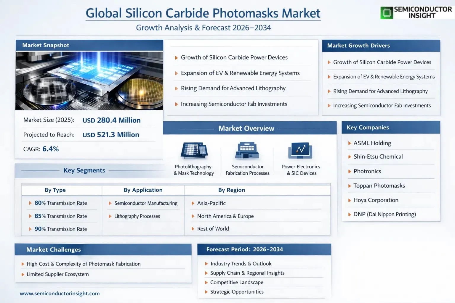
Silicon Carbide Photomasks market size was valued at USD 280.4 million in 2025. The market is projected to grow from USD 298.6 million in 2026 to USD 521.3 million by 2034, exhibiting a CAGR of 6.4% during the forecast period.
Silicon Carbide Photomask is a critical material used in photolithography processes, typically deposited on the surface of a photomask or mask plate. Silicon carbide has high hardness, excellent thermal conductivity, and chemical resistance, making it suitable for use as an anti-reflective coating (ARC), hard mask layer, or other functional films that enhance the precision and stability of the lithography process. These photomasks are categorized by transmission rate, including 80% Transmission Rate, 85% Transmission Rate, 90% Transmission Rate, and other variants, each serving distinct requirements across semiconductor fabrication and advanced lithography applications.
The market is experiencing steady growth driven by the accelerating demand for advanced semiconductor chip manufacturing and the broader adoption of wide-bandgap semiconductor technologies. The rising integration of Silicon Carbide (SiC) components in electric vehicles (EVs), renewable energy systems, and high-frequency power electronics is significantly expanding downstream demand for precision photomask solutions. Furthermore, increasing investments in semiconductor fabrication infrastructure across Asia-Pacific , particularly in China, Japan, and South Korea , are reinforcing market momentum. Key global manufacturers operating in this space include ASML, Shin-Etsu, and FST, among others, who collectively held a substantial share of global revenues in 2025 and continue to drive product innovation and capacity expansion to meet evolving lithography requirements.
MARKET DRIVERS
Accelerating Adoption of Silicon Carbide in Power Electronics and Semiconductor Fabrication
The Silicon Carbide Photomasks Market is experiencing robust growth driven by the expanding deployment of silicon carbide (SiC) semiconductor devices across power electronics, electric vehicles (EVs), and industrial automation. SiC-based devices offer superior thermal conductivity, higher breakdown voltage, and improved switching efficiency compared to conventional silicon, making them indispensable in next-generation power conversion systems. As SiC wafer production scales up globally, the demand for high-precision photomasks tailored to SiC device geometries has intensified considerably. Photomasks are critical in defining the intricate circuit patterns during the photolithography process, and for SiC fabrication, these masks must meet exceptionally tight dimensional tolerances due to the material’s unique crystalline properties.
EV Revolution and Renewable Energy Infrastructure Fueling SiC Device Demand
A principal market driver for the Silicon Carbide Photomasks Market is the unprecedented growth trajectory of the electric vehicle industry and its associated charging infrastructure. Leading automotive OEMs and Tier-1 suppliers are transitioning inverter and onboard charger designs from silicon IGBTs to SiC MOSFETs, substantially improving energy efficiency. This transition is compelling SiC device manufacturers to ramp production volumes and invest in advanced photomask technologies capable of supporting tighter design rules. Simultaneously, the global push toward solar inverters, wind energy converters, and smart grid systems is generating parallel demand for high-voltage SiC components, which in turn reinforces procurement activity within the photomask supply chain.
➤ The global shift toward wide-bandgap semiconductors, particularly silicon carbide, is creating sustained demand for advanced photomask solutions capable of supporting sub-micron patterning requirements in high-temperature and high-frequency device applications.
Furthermore, increasing government-backed semiconductor self-sufficiency programs across North America, Europe, and Asia-Pacific are catalyzing investments in SiC fabrication facilities. Incentive frameworks such as the U.S. CHIPS and Science Act and the European Chips Act are directing capital toward domestic SiC device manufacturing ecosystems, thereby generating a structured pipeline of demand for photomask suppliers. As foundries expand their SiC process node capabilities, photomask procurement cycles are becoming more frequent and technically demanding, reinforcing the long-term growth dynamics of the Silicon Carbide Photomasks Market.
MARKET CHALLENGES
Technical Complexity of Photomask Fabrication for Silicon Carbide Process Nodes
One of the foremost challenges confronting the Silicon Carbide Photomasks Market is the inherent technical complexity associated with producing photomasks that meet the precision demands of SiC device fabrication. Unlike conventional silicon-based processes, SiC device manufacturing involves higher process temperatures, specific doping profiles, and unique etch chemistry requirements that impose stringent specifications on photomask materials and pattern fidelity. Even marginal defects or dimensional inaccuracies in the photomask can result in catastrophic yield losses during SiC wafer processing, given the material’s sensitivity to structural imperfections. This necessitates photomask manufacturers to deploy advanced electron-beam (e-beam) writing systems and multi-layer phase-shift mask technologies, both of which involve significant capital investment and highly specialized process expertise.
Other Challenges
High Capital Expenditure and Long Lead Times
The production of photomasks for SiC applications demands state-of-the-art lithography equipment, ultra-pure quartz substrates, and cleanroom environments with contamination control at sub-nanometer levels. These prerequisites translate into elevated capital expenditure requirements for photomask manufacturers, creating high barriers to entry and limiting the number of qualified suppliers capable of serving the Silicon Carbide Photomasks Market. Consequently, procurement lead times for advanced SiC photomasks can extend significantly, creating supply bottlenecks for SiC device manufacturers seeking to scale production rapidly.
Limited Supplier Ecosystem and Concentration Risk
The global photomask supply chain for SiC applications remains relatively concentrated among a limited number of established vendors with the technical capability to serve advanced SiC node requirements. This concentration introduces supply chain vulnerability, as disruptions at key manufacturing sites , whether from natural events, geopolitical tensions, or raw material shortages , can adversely impact the broader SiC device production ecosystem. Diversifying the photomask supplier base remains a persistent strategic priority for SiC foundries and IDMs operating within this market.
MARKET RESTRAINTS
Elevated Production Costs and Substrate Material Constraints Limiting Market Scalability
A significant restraint on the Silicon Carbide Photomasks Market is the persistently high cost structure associated with photomask production for SiC applications. Advanced SiC photomasks require specialized quartz or low thermal expansion (LTE) glass substrates, precision chrome or molybdenum silicide absorber layers, and sophisticated anti-reflective coatings, all of which contribute to elevated per-unit costs relative to standard silicon photomasks. These cost dynamics compress the margin flexibility of photomask suppliers and present procurement budget challenges for smaller SiC device manufacturers and fabless design companies operating in cost-sensitive market segments.
Technological Transition Risks Associated with Next-Generation Lithography Adoption
The ongoing industry transition toward extreme ultraviolet (EUV) lithography and multi-patterning techniques introduces a layer of technological uncertainty that acts as a restraint on near-term investment decisions within the Silicon Carbide Photomasks Market. While current SiC device fabrication predominantly utilizes deep ultraviolet (DUV) lithography, the anticipated migration toward finer process nodes may require photomask suppliers to undertake significant retooling and process redevelopment. The capital-intensive nature of this transition, combined with uncertainty surrounding the timing of widespread EUV adoption in SiC fabs, creates hesitancy among photomask manufacturers to commit prematurely to next-generation infrastructure investments, thereby temporarily constraining capacity expansion within the market.
MARKET OPPORTUNITIES
Expansion of SiC Power Device Manufacturing Creating Long-Term Photomask Demand
The Silicon Carbide Photomasks Market stands to benefit substantially from the planned capacity expansions being undertaken by major SiC wafer and device manufacturers across North America, Europe, and Asia. Announcements of greenfield SiC wafer fabrication facilities and capacity upgrade programs at established fabs signal a structural increase in photomask demand over the coming years. Each new SiC production line requires a comprehensive library of qualified photomasks across multiple device layers, and the transition to larger wafer diameters , from 150mm to 200mm , necessitates the development of entirely new photomask sets compatible with the expanded wafer format. This generational wafer size transition represents a discrete and substantial opportunity for photomask suppliers to expand their product portfolios and capture new design-in engagements.
Emerging Applications in 5G Infrastructure, Aerospace, and Defense Sectors
Beyond automotive and industrial power electronics, the Silicon Carbide Photomasks Market is poised to benefit from the growing adoption of SiC devices in 5G base station infrastructure, RF power amplifiers, aerospace avionics, and defense electronics. These application segments demand SiC components with highly customized device architectures and specialized process flows, creating requirements for bespoke photomask solutions with tight tolerances and application-specific pattern designs. As defense agencies and commercial 5G network operators increase procurement of high-frequency SiC-based components, photomask suppliers with technical expertise in compound semiconductor patterning will be strategically positioned to capture high-value, low-volume but margin-accretive contracts within the Silicon Carbide Photomasks Market ecosystem.
Digitalization of Photomask Design and AI-Driven Defect Inspection Technologies
The integration of artificial intelligence and machine learning into photomask design verification, optical proximity correction (OPC), and automated defect inspection workflows represents a transformative opportunity for participants in the Silicon Carbide Photomasks Market. AI-powered inspection platforms are demonstrably improving defect detection sensitivity and throughput at photomask production facilities, reducing cycle times and lowering the incidence of mask-related yield excursions at SiC fabs. Photomask suppliers that invest in AI-augmented process control and digital twin simulation capabilities will gain a meaningful competitive differentiation advantage, enabling them to offer faster qualification cycles and improved mask lifetime performance , attributes increasingly valued by SiC device manufacturers operating under aggressive production ramp schedules.
MAIN TITLE HERE () Trends
Growing Adoption of Silicon Carbide Photomasks in Advanced Semiconductor Lithography
The Silicon Carbide Photomasks Market is experiencing notable momentum driven by the rapid expansion of power electronics and wide-bandgap semiconductor fabrication. As semiconductor manufacturers intensify their focus on precision lithography for next-generation devices, silicon carbide photomasks have emerged as a preferred solution due to their superior hardness, thermal conductivity, and chemical resistance. These properties make SiC-based photomasks particularly effective as hard mask layers and anti-reflective coatings (ARC), enabling tighter pattern fidelity and greater process stability across high-volume manufacturing environments.
The increasing deployment of silicon carbide in electric vehicles (EVs), renewable energy inverters, and industrial power systems is generating sustained upstream demand for high-quality SiC photomasks. Semiconductor chip manufacturers are scaling up SiC wafer production, which directly intensifies the requirement for photomasks capable of withstanding aggressive lithography cycles without dimensional degradation. This dynamic is reshaping procurement strategies across leading foundries and integrated device manufacturers globally.
Other Trends
Rising Demand for High Transmission Rate Photomasks
Within the Silicon Carbide Photomasks Market, product segments defined by transmission rate , including 80%, 85%, and 90% transmission variants , are witnessing differentiated growth trajectories. Higher transmission rate photomasks are increasingly favored in cutting-edge lithography nodes where light uniformity and minimal optical loss are critical. Manufacturers are investing in process refinements to produce photomasks with consistent transmission performance, responding to the tightening specifications demanded by semiconductor chip manufacturing applications.
Concentration Among Key Global Manufacturers
The competitive landscape of the Silicon Carbide Photomasks Market remains relatively consolidated, with leading players such as ASML, Shin-Etsu, and FST maintaining significant influence over global supply. These companies are actively pursuing product development initiatives and capacity expansions to address growing demand from lithography and semiconductor chip manufacturing end-users. Their dominance reflects both the technical barriers to entry and the importance of established quality certifications in this precision materials segment.
Regional Dynamics Shaping the Silicon Carbide Photomasks Market Outlook
Asia, led by China, Japan, and South Korea, represents the most active regional market for silicon carbide photomasks, supported by large-scale semiconductor fabrication infrastructure and aggressive government-backed investment in domestic chip production. North America, particularly the United States, remains a critical innovation hub where advanced lithography research and SiC device commercialization are accelerating adoption. Europe is also gaining traction, with Germany and other industrial economies integrating SiC-based power components into automotive and energy systems. These regional trends collectively underscore the expanding global footprint of the Silicon Carbide Photomasks Market across diverse application verticals.
COMPETITIVE LANDSCAPE
Key Industry Players
Silicon Carbide Photomasks Market – Competitive Dynamics, Strategic Positioning, and Leading Manufacturer Profiles
Silicon Carbide Photomasks market is characterized by a moderately consolidated competitive structure, with a handful of technologically advanced players commanding a significant share of global revenues. These companies leverage deep expertise in photolithography materials, precision thin-film deposition, and semiconductor-grade quality control to maintain their market positioning. Leading manufacturers such as ASML and Shin-Etsu Chemical have established themselves as dominant forces, benefiting from extensive R&D capabilities, long-standing relationships with major semiconductor fabs, and robust intellectual property portfolios. The top five global players collectively accounted for a notable share of total market revenue in 2025, underscoring the high barriers to entry defined by capital-intensive manufacturing processes, stringent purity requirements, and the technical complexity of producing silicon carbide-based photomask coatings with precise transmission rate specifications , including 80%, 85%, and 90% transmission rate variants , used across lithography and semiconductor chip manufacturing applications.
Beyond the market leaders, a growing number of specialized and regional players are carving out meaningful niches within the Silicon Carbide Photomasks ecosystem. Companies such as FST and other Asia-Pacific-based manufacturers are increasingly investing in advanced SiC coating technologies to serve the rapidly expanding semiconductor industries in China, South Korea, Japan, and Southeast Asia. European and North American suppliers are also focusing on innovation in anti-reflective coating (ARC) formulations and hard mask layer development to meet the evolving demands of next-generation chip fabrication nodes. Strategic mergers, acquisitions, and technology partnerships are reshaping the competitive landscape, as companies seek to expand their geographic footprint, broaden their product portfolios, and strengthen supply chain resilience. Market participants are also responding to rising demand from EV power electronics and wide-bandgap semiconductor applications, further intensifying competitive activity across the value chain.
List of Key Silicon Carbide Photomasks Companies Profiled
- ASML Holding N.V.
- Shin-Etsu Chemical Co., Ltd.
- Photronics, Inc.
- Toppan Photomasks, Inc.
- FST Corporation
- Hoya Corporation
- SK Siltron Co., Ltd.
- DNP (Dai Nippon Printing Co., Ltd.)
- LG Innotek Co., Ltd.
- Advanced Reproductions Corporation
- Taiwan Mask Corporation
- Shenzhen Qingyi Photomask Limited
- Compugraphics International Ltd.
- Nippon Filcon Co., Ltd.
- Crytur, spol. s r.o.
Segment Analysis:
| Segment Category | Sub-Segments | Key Insights |
| By Type |
|
90% Transmission Rate is the leading segment within the Silicon Carbide Photomasks market by type, driven by its superior optical clarity and alignment with next-generation lithography demands.
|
| By Application |
|
Semiconductor Chip Manufacturing represents the dominant application segment, underpinned by the rapid expansion of global semiconductor fabrication capacity and surging demand for high-performance chips.
|
| By End User |
|
Foundries constitute the leading end-user segment, as global contract semiconductor manufacturing hubs operate at immense scales requiring a consistent and high-quality supply of advanced photomasks.
|
| By Coating Function |
|
Anti-Reflective Coating (ARC) is the leading functional segment, as the suppression of unwanted light reflection is paramount to achieving high-fidelity pattern transfer in advanced photolithography.
|
| By Technology Node |
|
Advanced Nodes (7nm–28nm) represent the leading technology node segment, as this range encompasses the bulk of current high-performance logic and power device production where SiC photomasks deliver the most compelling performance advantages.
|
Regional Analysis: Silicon Carbide Photomasks Market
Asia-Pacific
China is aggressively scaling its domestic silicon carbide photomask production capabilities as part of broader semiconductor self-sufficiency initiatives. Strong government subsidies and strategic industrial planning have encouraged local manufacturers to develop in-house photomask solutions for SiC power devices, reducing reliance on foreign suppliers and positioning the country as a critical force within the Asia-Pacific silicon carbide photomasks landscape.
Japan and South Korea bring decades of photomask precision engineering expertise to the Silicon Carbide Photomasks Market. Leading manufacturers in these countries have developed specialized mask chemistries and inspection technologies suited to the unique properties of SiC substrates. Their focus on yield improvement and defect minimization establishes them as premium suppliers serving both regional and global semiconductor fabrication clients.
Taiwan’s world-class semiconductor foundry infrastructure is increasingly integrating silicon carbide process flows, generating sustained demand for high-quality photomasks. As leading Taiwanese foundries expand their SiC device offerings for automotive and industrial customers, photomask suppliers are responding with customized solutions that address the stringent dimensional and defect tolerance requirements inherent to wide-bandgap semiconductor manufacturing.
India and select Southeast Asian nations are emerging as nascent contributors to the regional Silicon Carbide Photomasks Market. Policy-driven semiconductor incentive programs and growing interest in power electronics manufacturing are beginning to attract investment in SiC-related fabrication infrastructure. While still in early development stages, these markets represent a significant long-term growth opportunity for photomask suppliers seeking to diversify their regional customer base.
North America
North America represents one of the most technologically advanced markets for silicon carbide photomasks, underpinned by a strong ecosystem of semiconductor companies, research institutions, and defense-related electronics manufacturers. The United States, in particular, is home to several pioneering silicon carbide device developers and photomask solution providers whose innovations continue to shape global industry standards. Demand from the electric vehicle sector, aerospace applications, and grid-scale energy infrastructure has created a sustained pull for high-performance SiC photomasks capable of supporting next-generation power conversion systems. Federal initiatives aimed at strengthening domestic semiconductor supply chains have further catalyzed investment in advanced photomask capabilities. Canada also contributes through research collaborations and emerging cleantech applications. The North American Silicon Carbide Photomasks Market is characterized by a strong emphasis on intellectual property development, technology licensing, and close collaboration between photomask manufacturers and device designers to address increasingly complex process nodes.
Europe
Europe occupies a strategically important position in Silicon Carbide Photomasks market, with demand propelled by the region’s leadership in automotive electrification, industrial automation, and energy transition technologies. Germany, France, and the Netherlands are particularly active in advancing silicon carbide device manufacturing for EV powertrains and smart grid applications, creating consistent demand for precision photomasks. European semiconductor policy frameworks, including major public-private investment programs, are supporting the expansion of domestic SiC fabrication capacity, which in turn drives the need for locally sourced or regionally aligned photomask supply chains. The region’s stringent quality standards and emphasis on environmental sustainability also influence photomask manufacturing processes, encouraging the development of cleaner production methods. Collaborative research programs between academic institutions and industry players continue to push the boundaries of SiC photomask performance across critical application areas.
South America
South America presents a developing but promising frontier within Silicon Carbide Photomasks market. Brazil leads regional activity, with growing interest in renewable energy systems and industrial electronics creating an indirect demand pathway for silicon carbide-based power devices and associated photomask technologies. While the region currently lacks a substantial domestic semiconductor manufacturing base, increasing foreign direct investment in electronics and energy infrastructure is gradually building the foundations for future SiC technology adoption. Regional trade agreements and technology transfer initiatives are expected to facilitate deeper integration with global silicon carbide supply chains over the coming years. As local industries mature and electrification projects scale across energy, transportation, and industrial sectors, South America is anticipated to become a more active participant in the broader Silicon Carbide Photomasks Market ecosystem.
Middle East & Africa
The Middle East and Africa region currently occupies an early-stage position in the Silicon Carbide Photomasks Market, yet several structural factors point toward gradual growth in relevance over the forecast period. In the Middle East, ambitious economic diversification programs , particularly those focused on high-technology manufacturing and renewable energy , are beginning to stimulate interest in advanced semiconductor materials, including silicon carbide. The UAE and Saudi Arabia are investing in smart infrastructure and clean energy systems where SiC power devices offer efficiency advantages. Africa, while at a more nascent stage, is witnessing early-phase technology adoption in solar energy and telecommunications that could eventually create downstream demand for SiC-enabled components. As regional investments in semiconductor education, infrastructure, and manufacturing partnerships continue to develop, the Middle East and Africa are expected to progressively increase their engagement with Silicon Carbide Photomasks market.
Report Scope
This market research report provides a comprehensive analysis of the Silicon Carbide Photomasks Market, covering the forecast period 2026–2034. It offers detailed insights into market dynamics, technological advancements, competitive landscape, and key trends shaping the industry.
Key focus areas of the report include:
- Market Overview: The report begins with an overview outlining its current market scenario, key growth indicators, and industry transformation drivers. It discusses macroeconomic factors, demand–supply balance, regulatory landscape, and the strategic role of semiconductors in powering advancements across industries such as automotive, telecommunications, consumer electronics, and industrial automation.
- Market Size & Forecast: Historical data and future projections for revenue, unit shipments, and market value across major regions and segments.
- Segmentation Analysis: Detailed breakdown by product type, technology, application, and end-user industry to identify high-growth segments and investment opportunities.
- Regional Insights: Insights into market performance across North America, Europe, Asia-Pacific, Latin America, and the Middle East & Africa, including country-level analysis where relevant.
- Competitive Landscape: Profiles of leading market participants, including their product offerings, R&D focus, manufacturing capacity, pricing strategies, and recent developments such as mergers, acquisitions, and partnerships.
- Technology Trends & Innovation: Assessment of emerging technologies, integration of AI/IoT, semiconductor design trends, fabrication techniques, and evolving industry standards.
- Market Drivers & Restraints: Evaluation of factors driving market growth along with challenges, supply chain constraints, regulatory issues, and market-entry barriers.
- Stakeholder Insights: Insights for component suppliers, OEMs, system integrators, investors, and policymakers regarding the evolving ecosystem and strategic opportunities.
Primary and secondary research methods are employed, including interviews with industry experts, data from verified sources, and real-time market intelligence to ensure the accuracy and reliability of the insights presented.
FREQUENTLY ASKED QUESTIONS:
What is the current market size of Silicon Carbide Photomasks Market?
-> Global Silicon Carbide Photomasks Market was valued at USD 280.4 million in 2025 and is expected to reach USD 521.3 million by 2034, growing at a steady CAGR of 6.4% during the forecast period 2026–2034.
Which key companies operate in Silicon Carbide Photomasks Market?
-> Key players include ASML, Shin-Etsu, FST, among others. In 2025, the global top five players held approximately a significant share in terms of revenue in Silicon Carbide Photomasks market.
What are the key growth drivers?
-> Key growth drivers include rising demand for photolithography processes in semiconductor chip manufacturing, increasing adoption of Silicon Carbide Photomasks as anti-reflective coating (ARC) and hard mask layers, and expanding applications in lithography and semiconductor fabrication. The high hardness, excellent thermal conductivity, and chemical resistance of silicon carbide make it a preferred material for precision lithography.
Which region dominates the market?
-> Asia is a dominant region in the Silicon Carbide Photomasks Market, with China representing a significant country-level market. North America, particularly the U.S., also holds a notable market position, with the U.S. market estimated at USD million in 2025 and China projected to reach USD million during the forecast period.
What are the emerging trends?
-> Emerging trends include increasing use of Silicon Carbide as functional films in advanced photolithography, growing demand from semiconductor chip manufacturing and lithography applications, and rising adoption of 80%, 85%, and 90% transmission rate photomasks. The 80% Transmission Rate segment is projected to reach USD million by 2034, reflecting strong growth momentum in the coming years.

Get Sample Report PDF for Exclusive Insights
Report Sample Includes
- Table of Contents
- List of Tables & Figures
- Charts, Research Methodology, and more...