
Silicon Bridge Die for AI Multi-Chip Modules Market Insights
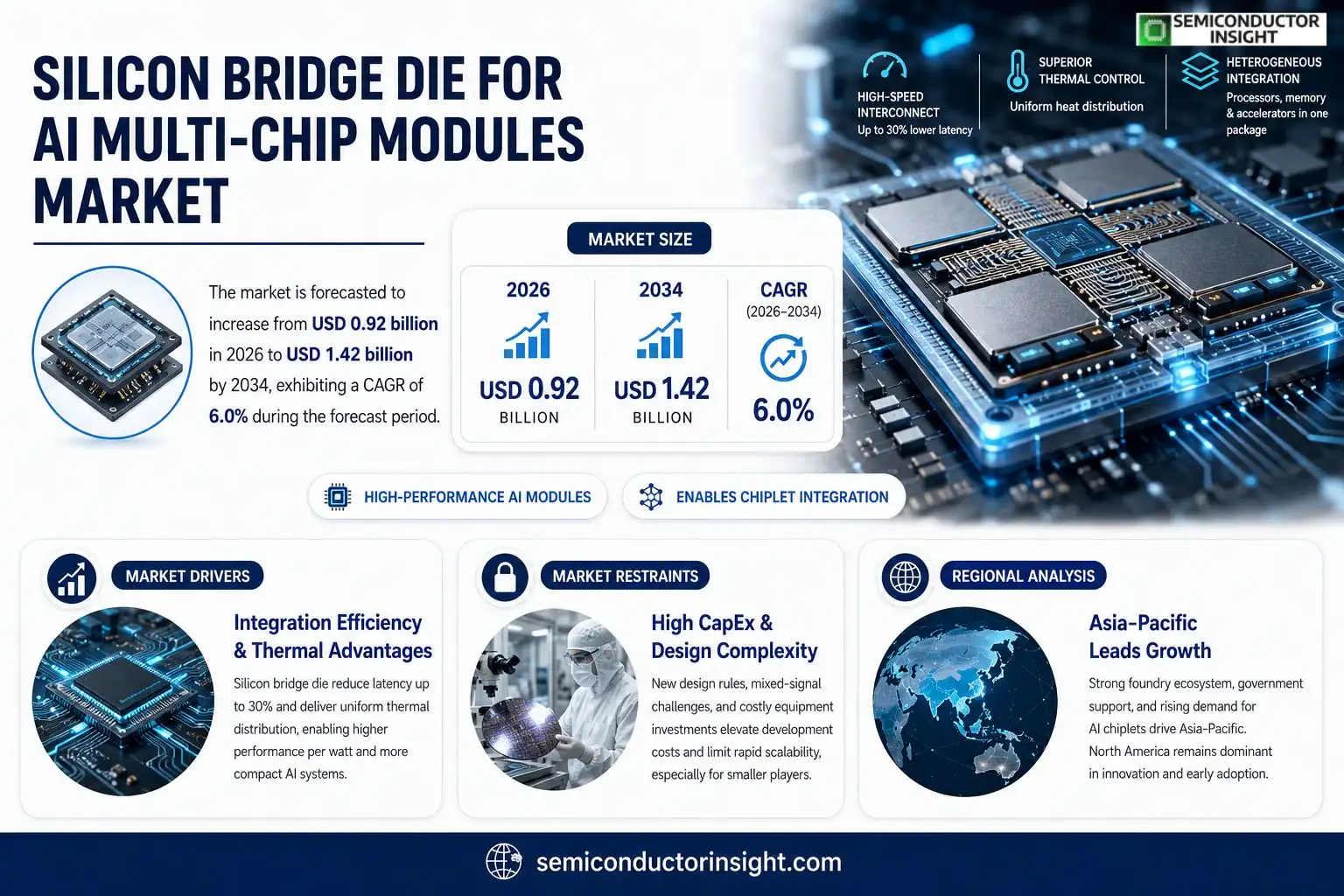
silicon bridge die for AI multi‑chip modules market size was valued at USD 0.85 billion in 2025 and is forecasted to increase from USD 0.92 billion in 2026 to USD 1.42 billion by 2034, exhibiting a CAGR of 6.0% during the forecast period.
Silicon bridge dies are ultra‑thin interconnect substrates that enable heterogeneous integration of multiple AI chips within a single package. By providing high‑density electrical pathways and thermal management across disparate dies, they allow designers to combine processors, memory stacks and specialized accelerators without incurring the latency penalties of traditional board‑level connections.The expansion of this segment reflects several dynamics: rising capital spending on edge‑AI hardware, growing adoption of chiplet architectures in data‑center accelerators, and continuous improvements in wafer‑level packaging that lower cost per gigaflop. Recent collaborations illustrate this trendfor example, TSMC announced a joint development program with Nvidia in early 2024 aimed at scaling silicon bridge technology for next‑generation GPU chiplets; Intel’s Advanced Packaging Group introduced a new bridge‑die offering that supports heterogeneous integration of Habana Labs inference engines; Samsung Electronics reported volume shipments of its bridge‑die based AI modules later this year.
MARKET DRIVERS
Integration Efficiency Gains
Manufacturers are increasingly valuing the ability of silicon bridge die to collapse the physical distance between AI accelerators and memory dies. By replacing traditional package‑on‑package approaches, the bridge die cuts signal latency by up to 30 % and reduces power draw on the board. These engineering savings translate directly into higher performance per watt, a metric that AI hardware designers monitor closely.
Thermal Management Advantages
Because the bridge die consolidates interconnects into a thin silicon layer, heat generation is more uniform across the module. This uniformity eases the burden on cooling solutions, allowing OEMs to deploy smaller heatsinks while maintaining safe operating temperatures. Improved thermal headroom enables higher clock rates without crossing reliability thresholds.
➤ The adoption of silicon bridge die accelerates data throughput across heterogeneous chips, creating a competitive edge for early adopters.
From a business perspective, the combined latency and thermal benefits lower the total cost of ownership for AI platforms. System integrators can offer slimmer, higher‑density products, which in turn opens up new form‑factor opportunities in data‑center edge nodes and autonomous‑vehicle racks. The cumulative effect is a stronger value proposition for customers seeking to differentiate on speed and efficiency.
MARKET CHALLENGES
Design Complexity Hurdles
Engineering teams must master a new stack of design rules that span analog, digital, and photonic domains. The bridge die introduces mixed‑signal considerations that are not present in conventional interposers, requiring deeper simulation cycles and tighter verification windows. Project timelines can extend by 10‑15 %, pressuring budgets and resource allocation.
Other Challenges
Manufacturing Yield Issues
Yield data from pilot runs indicate that minor variations in silicon thickness can cause impedance mismatches, leading to defective units. Addressing these defects demands tighter process controls and additional inspection steps, which raise per‑unit cost and may deter cost‑sensitive adopters.
MARKET RESTRAINTS
Capital Expenditure Barriers
Implementing silicon bridge die requires a substantial upfront investment in new lithography equipment and specialized probe stations. For fabs operating near capacity, reallocating wafer real‑estate to bridge die production can delay other high‑margin product lines. The financial hurdle limits rapid scaling, especially among smaller foundries that lack deep pockets.
MARKET OPPORTUNITIES
Emerging Edge‑AI Deployments
Edge servers destined for smart‑city sensors, industrial IoT gateways, and autonomous‑driving platforms demand compact AI compute with minimal latency. Silicon bridge die enable multi‑chip stacks that fit within a 20 mm × 20 mm footprint while delivering the throughput required for real‑time inference. Companies that secure early supply contracts stand to capture a sizable share of the rapidly forming edge‑AI ecosystem.Furthermore, the convergence of 3‑D packaging standards and AI‑specific silicon roadmaps creates a fertile ground for co‑development partnerships. Vendors that align their bridge‑die offerings with next‑generation AI cores can embed differentiation directly into the silicon layer, opening licensing revenue streams and reinforcing ecosystem lock‑in.
Silicon Bridge Die for AI Multi-Chip Modules Market Trends
Heterogeneous Integration Gains Traction
The ability of silicon bridge dies to stitch together disparate AI engines inside a single package has reshaped design calculations for both edge devices and data‑center accelerators. Designers now rely on the ultra‑thin substrate to route high‑density signals while preserving signal integrity, which cuts board‑level latency and reduces the bill of materials. The market’s valuation of USD 0.85 billion in 2025 and the lift to USD 1.42 billion by 2034 illustrate how customers are willing to invest in packaging solutions that free up silicon real estate for algorithmic advances. This shift reflects a pragmatic response to the rising cost per gigaflop of monolithic chips, prompting system architects to favor modular builds that can be upgraded piece by piece.
Other Trends
Supply Chain Consolidation
Recent joint programs have signaled a move toward tighter coordination among foundries, AI chip designers, and packaging firms. Early‑2024 TSMC’s collaboration with Nvidia aimed at scaling bridge technology for next‑generation GPU chiplets, while Intel’s Advanced Packaging Group launched a bridge‑die variant optimized for Habana Labs inference engines. Samsung’s volume shipments of bridge‑die‑based AI modules later in the year confirmed that large‑scale production is no longer a pilot effort but a regular supply‑chain activity. These alliances reduce time‑to‑market for new AI solutions and create a predictable pipeline that benefits OEMs seeking to differentiate product lines without bearing the full risk of new silicon development.
Thermal Management Advances
Beyond electrical performance, the thermal profile of densely packed AI chiplets has become a decisive factor in module selection. Silicon bridge dies now incorporate embedded micro‑heat spreaders and low‑thermal‑resistance paths that dissipate heat more uniformly across the stack. This capability enables higher power densities, allowing a single module to host multiple accelerator dies while staying within envelope temperature limits. For system integrators, the result is a broader design window for form‑factor constrained products such as autonomous‑vehicle processors and compact edge inferencing boxes. As manufacturers continue to refine wafer‑level packaging processes, the cost advantage of these thermal solutions is expected to improve, prompting more enterprises to adopt bridge‑die architectures as a standard building block for future AI hardware.
COMPETITIVE LANDSCAPEKey Industry Players
Competitive dynamics in the silicon bridge die ecosystem for AI multi‑chip modules
The silicon bridge die segment is anchored by three manufacturers that collectively command the bulk of shipments. TSMC leverages its leading wafer‑level packaging capacity to supply bridge dies for Nvidia’s chiplet‑based GPUs, while Intel’s Advanced Packaging Group has rolled out a bridge‑die line that integrates Habana Labs inference engines directly into its data‑center accelerators. Samsung complements the trio by moving from pilot runs to volume production, exporting bridge‑die‑based AI modules to tier‑1 OEMs. Their dominance stems from deep investments in lithography, strong IP portfolios, and the ability to bundle bridge dies with proprietary interconnect standards, which gives customers a low‑risk path to heterogeneous integration.Beyond the top tier, a cluster of specialized firms sustains the ecosystem’s breadth. ASE Technology and Amkor provide foundry‑agnostic bridge‑die services that appeal to niche designers seeking flexible form‑factors. Foundries and STMicroelectronics focus on automotive‑grade reliability, positioning bridge dies for edge‑AI deployments in vehicles. Infineon targets power‑sensitive applications, while Qualcomm and AMD (via Xilinx) exploit bridge‑die technology to assemble heterogeneous SoCs for 5G and high‑performance computing. Marvell, Broadcom, ON Semiconductor, and Imagination Technologies round out the landscape, each offering targeted solutionsranging from networking accelerators to graphics‑centric AI enginesthat keep the market diversified and responsive to emerging workloads.
List of Key Silicon Bridge Die for AI Multi‑Chip Modules Companies Profiled
- TSMC
- Intel
- Samsung Electronics
- ASE Technology Holding
- Amkor Technology
- Foundries
- STMicroelectronics
- Infineon Technologies
- Qualcomm
- AMD (Xilinx)
- Marvell Technology
- Broadcom
- ON Semiconductor
- Imagination Technologies (PowerVR)
Segment Analysis:
| Segment Category | Sub-Segments | Key Insights |
| By Type |
|
Passive Silicon Bridge Die
|
| By Application |
|
Edge‑AI Accelerators
|
| By End User |
|
AI Chip Designers
|
Regional Analysis: Silicon Bridge Die for AI Multi-Chip Modules Market
North America
The concentration of silicon design firms in Silicon Valley and Austin creates a network effect where design tools, IP cores, and verification services co‑locate. This proximity accelerates collaborative iterations on bridge‑die topologies, allowing firms to refine interconnect strategies faster than dispersed competitors. The resulting rapid feedback loop nurtures a culture of continuous improvement that fuels market leadership.
A deep reservoir of engineers trained in 3‑D integration, RF packaging, and high‑density interconnects supplies the region with a unique skill set. Universities such as MIT, Stanford, and Carnegie Mellon embed bridge‑die concepts into curricula, ensuring fresh graduates arrive with practical know‑how. Companies leverage this talent pool to shorten development cycles and differentiate their product roadmaps.
Capital availability in the United States remains robust, with venture funds and corporate investors earmarking resources for heterogeneous integration projects. Early‑stage financing often targets proof‑of‑concept bridge‑die chips, while later rounds fund scaling of multi‑chip module fabs. This layered funding structure gives firms the financial runway to iterate designs without compromising long‑term strategic goals.
Policy programs such as the CHIPS Act and state‑level tax credits lower the effective cost of silicon R&D, encouraging firms to push the limits of bridge‑die density and power efficiency. These incentives also attract foreign design houses to set up R&D outposts, enriching the domestic ecosystem with perspectives and expanding collaborative opportunities.
Europe
Europe’s approach to the Silicon Bridge Die for AI Multi‑Chip Modules Market reflects a balance between ambitious research agendas and a fragmented manufacturing base. The presence of several leading consortia, such as the European Processor Initiative, channels public funding toward heterogeneous integration, fostering collaborative prototypes across borders. However, the absence of a unified fab capacity comparable to North America means many design firms rely on external foundries in Asia, which adds logistical complexity and extends time‑to‑market. Nonetheless, the region compensates with strong standards bodies that shape interconnect specifications, granting European players influence over design norms. As sustainability criteria become more prominent, European manufacturers are also pioneering low‑temperature bonding techniques that align with the region’s environmental directives.
Asia‑Pacific
Asia‑Pacific’s foothold in the Silicon Bridge Die for AI Multi‑Chip Modules Market stems from its dense cluster of fab capacity and aggressive government roadmaps. Countries such as Taiwan, South Korea, and Japan operate world‑class silicon foundries that have adapted their process lines to accommodate heterogeneous die‑stacking, offering designers a rapid path from prototype to volume production. National AI strategies prioritize integration technologies, prompting subsidies for bridge‑die research labs. While the region excels in manufacturing throughput, challenges arise in aligning design standards across jurisdictions, which can impede cross‑border collaboration. Nevertheless, the sheer scale of production and the willingness to invest in next‑generation packaging position Asia‑Pacific as a decisive engine for market expansion.
South America
South America’s participation in the Silicon Bridge Die for AI Multi‑Chip Modules Market remains nascent but is gaining momentum through targeted university‑industry partnerships. Brazil’s leading research institutes have begun to explore heterogeneous integration as part of broader digital transformation agendas, attracting modest venture capital interested in localized AI hardware. The region’s primary obstacle is limited domestic fab capability, compelling designers to depend on offshore production, which raises cost and latency considerations. However, emerging policy incentives that promote high‑tech clusters in São Paulo and Buenos Aires aim to cultivate a skilled workforce and attract multinational R&D centers. Over the next few years, these initiatives could elevate South America from peripheral observer to a collaborative contributor.
Middle East & Africa
The Middle East & Africa region is carving a niche in the Silicon Bridge Die for AI Multi‑Chip Modules Market by leveraging sovereign wealth funds to back strategic technology hubs. The United Arab Emirates and Saudi Arabia have announced dedicated programs that subsidize design talent and import advanced packaging equipment, aiming to reduce reliance on external supply chains. While indigenous fab infrastructure remains limited, partnerships with Asian manufacturers provide a conduit for prototype fabrication. Additionally, the region’s emphasis on smart city initiatives creates a demand for compact, high‑performance AI compute blocks, which bridge‑die solutions can satisfy. If fiscal support persists, the area may evolve into a valuable design and integration outpost for players.
Report Scope
This market research report provides a comprehensive analysis of the Silicon Bridge Die for AI Multi-Chip Modules Market , covering the forecast period 2026–2034. It offers detailed insights into market dynamics, technological advancements, competitive landscape, and key trends shaping the industry.
Key focus areas of the report include:
- Market Overview: The report begins with an overview outlining its current market scenario, key growth indicators, and industry transformation drivers. It discusses macroeconomic factors, demand–supply balance, regulatory landscape, and the strategic role of semiconductors in powering advancements across industries such as automotive, telecommunications, consumer electronics, and industrial automation.
- Market Size & Forecast: Historical data and future projections for revenue, unit shipments, and market value across major regions and segments.
- Segmentation Analysis: Detailed breakdown by product type, technology, application, and end-user industry to identify high-growth segments and investment opportunities.
- Regional Insights: Insights into market performance across North America, Europe, Asia-Pacific, Latin America, and the Middle East & Africa, including country-level analysis where relevant.
- Competitive Landscape: Profiles of leading market participants, including their product offerings, R&D focus, manufacturing capacity, pricing strategies, and recent developments such as mergers, acquisitions, and partnerships.
- Technology Trends & Innovation: Assessment of emerging technologies, integration of AI/IoT, semiconductor design trends, fabrication techniques, and evolving industry standards.
- Market Drivers & Restraints: Evaluation of factors driving market growth along with challenges, supply chain constraints, regulatory issues, and market-entry barriers.
- Stakeholder Insights: Insights for component suppliers, OEMs, system integrators, investors, and policymakers regarding the evolving ecosystem and strategic opportunities.
Primary and secondary research methods are employed, including interviews with industry experts, data from verified sources, and real-time market intelligence to ensure the accuracy and reliability of the insights presented.
FREQUENTLY ASKED QUESTIONS:
What is the current market size of Silicon Bridge Die for AI Multi-Chip Modules Market?
-> Silicon Bridge Die for AI Multi-Chip Modules Market was valued at USD 0.85 billion in 2025 and is expected to reach USD 1.42 billion by 2034, exhibiting a CAGR of 6.0% during the forecast period.
Which key companies operate in Silicon Bridge Die for AI Multi-Chip Modules Market?
-> Key players include TSMC, Nvidia, Intel, Samsung Electronics, ASE Group, and Amkor Technology, among others.
What are the key growth drivers?
-> Key growth drivers include rising capital spending on edge‑AI hardware, increasing adoption of chiplet architectures in data‑center accelerators, and continuous improvements in wafer‑level packaging that lower cost per gigaflop.
Which region dominates the market?
-> Asia-Pacific is the fastest‑growing region, while North America remains a dominant market due to strong semiconductor ecosystem and early‑stage adoption of advanced packaging.
What are the emerging trends?
-> Emerging trends include advanced heterogeneous integration platforms, AI‑driven design automation for chiplet ecosystems, 3D stacking techniques, and volume‑scaled bridge‑die shipments for next‑generation AI modules.
Get Sample Report PDF for Exclusive Insights
Report Sample Includes
- Table of Contents
- List of Tables & Figures
- Charts, Research Methodology, and more...
 Download Sample Report PDF



