
Semiconductor Yield Management Solutions Market Insights
Global Semiconductor Yield Management Solutions Market size was valued at USD 1.38 billion in 2025.
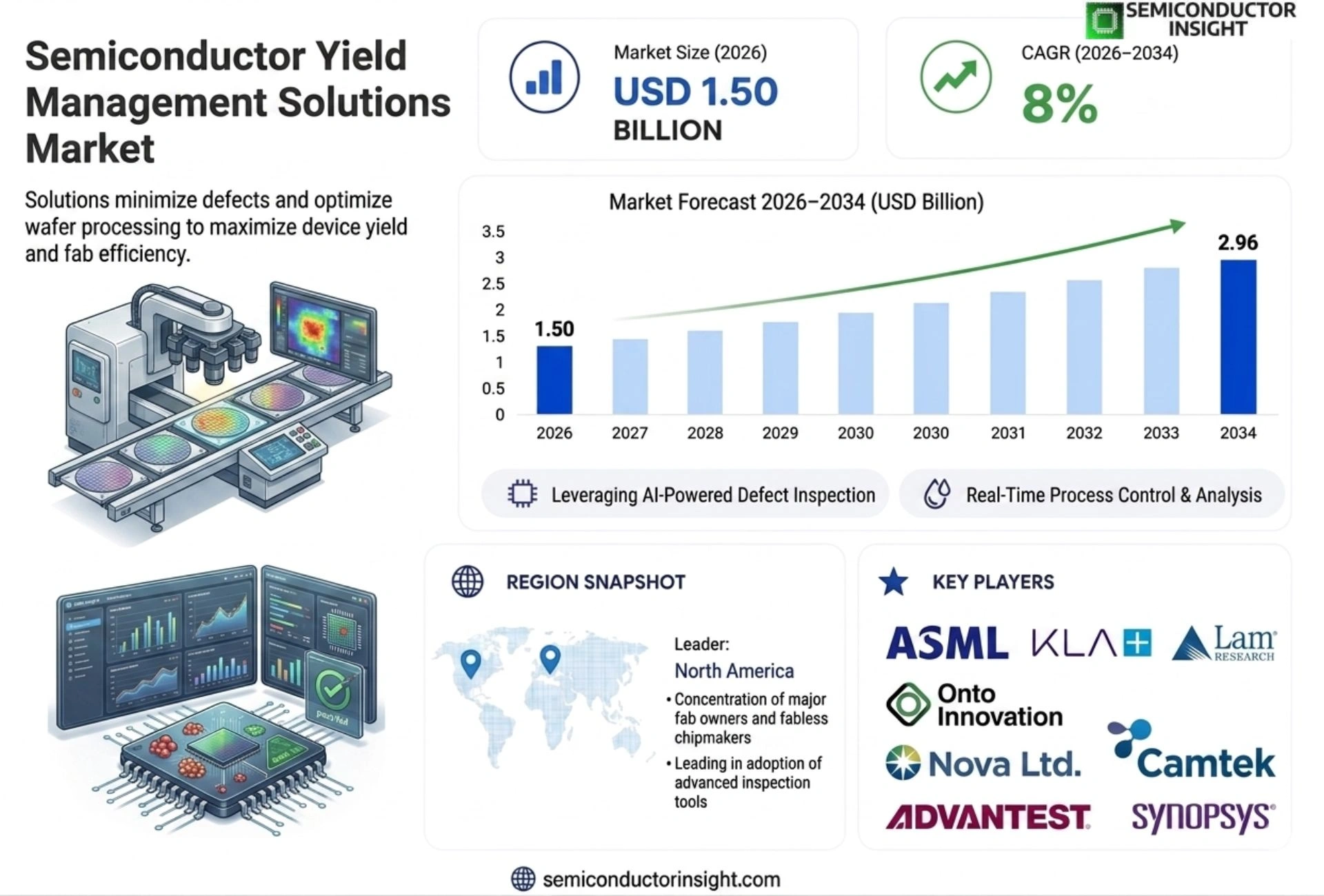
The market is projected to grow from USD 1.50 billion in 2026 to USD 2.96 billion by 2034, exhibiting a CAGR of 8% during the forecast period.
Semiconductor yield management solutions encompass integrated software platforms, advanced analytics tools, and specialized hardware modules that monitor, diagnose, and optimize wafer‑level production efficiency across lithography, etching, deposition and test stages.
These offerings employ machine‑learning algorithms for real‑time defect detection, predictive maintenance of equipment, and root‑cause analysis that together boost overall equipment effectiveness (OEE) while reducing scrap rates.
They also interface with manufacturing execution systems (MES) and enterprise resource planning (ERP) suites to provide end‑to‑end visibility across the fab.
The market is accelerating because chipmakers are scaling capacity for advanced nodes such as 3‑nm and beyond, intensifying pressure on defect density control.
Furthermore, heightened investment in AI‑driven analytics and government incentives supporting domestic semiconductor fabs are fueling demand for sophisticated yield management suites.
Key vendors,including Applied Materials Inc., KLA Corporation and ASML Holding N.V.,are expanding their portfolios through strategic acquisitions and partnerships that enhance data integration capabilities.
MARKET DRIVERS
Increasing Demand for Advanced Process Nodes
Semiconductor Yield Management Solutions Market is being propelled by the rapid adoption of sub‑10 nm process technologies, where even minor defects can translate into substantial revenue loss. Foundries reporting yield improvements of 3‑5 % have seen annual cost savings exceeding $150 million, underscoring the economic imperative for sophisticated yield analytics.
AI‑Driven Yield Analytics and Real‑Time Process Control
Machine‑learning platforms now enable predictive defect detection, allowing manufacturers to adjust lithography parameters on the fly. Companies that integrated AI‑based yield tools in 2022 achieved a 12 % faster time‑to‑market for new node introductions, reinforcing the competitive advantage of early adopters.
➤ Yield losses of 5‑10 % can erode up to $200 million annually for leading fabs, making advanced yield management a critical cost‑avoidance strategy.
Overall, the convergence of high‑performance computing workloads and the push for cost‑effective production is driving robust growth expectations for the market, with revenue projected to surpass $2.8 billion by 2030.
MARKET CHALLENGES
Complexity of Multi‑Pattern Integration
As device architectures evolve to incorporate heterogeneous integration, the variability across patterning steps intensifies. This complexity hampers the ability of traditional statistical process control methods to isolate root‑cause failures, creating a bottleneck for many mid‑size manufacturers.
Other Challenges
Cost Sensitivity
The high capital expenditure required for state‑of‑the‑art yield management platforms can deter budget‑constrained fabs, limiting widespread adoption despite clear long‑term ROI.
MARKET RESTRAINTS
Limited Availability of Skilled Personnel
Deploying advanced yield solutions demands expertise in data science, semiconductor physics, and equipment integration. The scarcity of professionals who can bridge these domains creates a talent gap, slowing implementation timelines and inflating operational costs for early movers.
MARKET OPPORTUNITIES
Emergence of Edge Computing and Specialized AI Chips
The surge in edge‑centric AI applications is prompting manufacturers to launch niche, low‑volume product lines with stringent yield requirements. Tailored yield management suites that offer rapid defect characterization for such specialized nodes present a high‑growth niche, projected to contribute over 20 % of incremental market value through 2030.
Semiconductor Yield Management Solutions Market Trends
Advanced Node Scaling Drives Yield Tool Adoption
Semiconductor Yield Management Solutions Market is experiencing a clear shift as chip manufacturers expand production at 3‑nm and smaller nodes. Tight defect budgets and the high cost per wafer make real‑time defect detection and predictive maintenance essential. Vendors are responding with integrated software platforms that embed machine‑learning models directly into fab equipment, allowing operators to intervene before a defect propagates across a lot. This trend improves overall equipment effectiveness while keeping scrap rates at historically low levels, reinforcing the strategic importance of yield management in advanced technology roadmaps.
Other Trends
Integration with MES and ERP Systems
Seamless data exchange between yield management suites and manufacturing execution systems (MES) or enterprise resource planning (ERP) solutions is becoming a baseline expectation. By linking wafer‑level analytics to production schedules, fabs can dynamically adjust lot sequencing, allocate resources more efficiently, and align yield insights with financial reporting. Recent product releases emphasize standardized OPC‑UA interfaces and cloud‑based data lakes, which reduce integration effort and support multi‑fab visibility for global semiconductor operations.
AI‑Driven Predictive Analytics Gain Traction
Artificial‑intelligence algorithms are now central to Semiconductor Yield Management Solutions Market, moving beyond simple statistical monitoring to proactive yield prediction. These models analyze historical defect patterns, equipment health logs, and process parameter drift to forecast potential yield loss weeks in advance. The resulting early warnings enable preventive maintenance and process retuning before loss materializes, delivering measurable reductions in downtime. As chipmakers invest in AI talent and infrastructure, the adoption curve for these predictive tools is expected to steepen, positioning them as a core component of next‑generation fab automation strategies.
COMPETITIVE LANDSCAPE
Key Industry Players
Semiconductor Yield Management Solutions Market: A Competitive Arena Driven by Advanced Analytics, AI Integration, and Strategic Portfolio Expansion
Semiconductor yield management solutions market is characterized by the presence of a handful of dominant, technology-intensive players who command significant market share through continuous innovation, strategic acquisitions, and deep integration with fab-level manufacturing infrastructure. KLA Corporation stands as the undisputed market leader, offering an expansive suite of process control, defect inspection, and yield management software platforms that are deeply embedded across leading-edge fabs globally. Applied Materials Inc. closely follows, leveraging its broad equipment portfolio and advanced analytics capabilities to deliver end-to-end yield optimization across lithography, etch, and deposition process nodes. ASML Holding N.V. reinforces its competitive position through its monopoly in extreme ultraviolet (EUV) lithography systems, which are increasingly integrated with yield management data loops critical for 3-nm and sub-3-nm node production. These top-tier players are aggressively expanding their portfolios through targeted acquisitions and cross-industry partnerships, aiming to enhance real-time defect detection, machine-learning-driven root-cause analysis, and seamless MES and ERP data integration across the fab ecosystem.
Beyond the dominant players, several specialized and mid-tier companies are carving out significant competitive positions by addressing niche segments within the semiconductor yield management solutions landscape. Synopsys and Cadence Design Systems provide robust electronic design automation and process simulation tools that directly influence wafer-level yield outcomes at the design stage. PDF Solutions and Onto Innovation have built strong reputations through advanced data analytics platforms and precision metrology solutions tailored specifically for yield enhancement workflows. Hitachi High-Tech Corporation and Rudolph Technologies (now part of Onto Innovation) contribute specialized inspection and metrology hardware that interfaces directly with yield management software suites. Meanwhile, companies such as Cohu Inc., Teradyne Inc., and Kulicke & Soffa Industries serve the back-end test and packaging segments, extending yield management capabilities beyond the wafer fab. Emerging vendors including Veeco Instruments, Inspectrology, and Nanometrics (now integrated into Onto Innovation) are further intensifying competition by delivering targeted, high-precision measurement and analysis solutions optimized for advanced semiconductor manufacturing nodes.
List of Key Semiconductor Yield Management Solutions Companies Profiled
- KLA Corporation
- Applied Materials Inc.
- ASML Holding N.V.
- Synopsys Inc.
- Cadence Design Systems Inc.
- PDF Solutions Inc.
- Onto Innovation Inc.
- Hitachi High-Tech Corporation
- Cohu Inc.
- Teradyne Inc.
- Kulicke & Soffa Industries Inc.
- Veeco Instruments Inc.
- Camtek Ltd.
- Rudolph Technologies Inc.
- Nanometrics Inc.
Segment Analysis:
| Segment Category | Sub-Segments | Key Insights |
| By Type |
|
Software‑centric Solutions dominate adoption because they enable rapid integration with existing fab workflows and provide scalable analytics capabilities.
|
| By Application |
|
Lithography‑focused Suites are perceived as critical enablers for sub‑10 nm productivity.
|
| By End User |
|
Fab Operators prioritize solutions that deliver end‑to‑end visibility and actionable insights.
|
| By Process Stage |
|
Wafer‑Fabrication Stage attracts the most sophisticated yield tools as defect control is paramount.
|
| By Solution Integration |
|
Integrated MES/ERP Suites are gaining traction as they reduce data silos and provide holistic operational insights.
|
Regional Analysis: North America
North America
The adoption of advanced analytics is rapidly transforming yield management, enabling manufacturers to identify patterns and predict potential yield issues proactively. This allows for timely interventions and minimizes costly downtime.
Artificial intelligence is playing an increasingly important role in optimizing manufacturing processes, leading to improvements in yield and resource utilization. AI algorithms can analyze vast amounts of data to identify optimal process parameters.
Real-time monitoring systems provide immediate insights into manufacturing processes, allowing for rapid detection and resolution of yield-related problems. This proactive approach is essential for maintaining high levels of production efficiency.
Implementing predictive maintenance strategies using data analytics helps to anticipate equipment failures before they occur, minimizing disruptions to the manufacturing process and maximizing yield.
North America
Semiconductor Yield Management Solutions Market in North America is fueled by the consistent demand from major semiconductor manufacturers operating in the United States, Canada, and Mexico. The focus on developing advanced microchips for various applications, including AI, automotive, and consumer electronics, drives the need for efficient yield management techniques. The region benefits from a robust ecosystem of technology providers, research institutions, and skilled engineers. Companies are increasingly looking towards integrated Semiconductor Yield Management Solutions to enhance their competitive edge. This proactive approach to yield optimization is essential for navigating the complexities of modern chip manufacturing. The emphasis on data-driven decision-making is a key driver for growth Semiconductor Yield Management Solutions Market.
Europe
Europe represents a significant portion of Semiconductor yield management solutions market, with a strong presence in countries like Germany, France, and the UK. The region’s emphasis on sustainable manufacturing and precision engineering aligns well with the requirements of advanced yield management tools. European manufacturers are actively adopting solutions to reduce waste and improve resource efficiency. The stringent regulatory environment and the focus on quality further drive the demand for sophisticated Semiconductor Yield Management Solutions. Innovation in this space is focused on energy efficiency and minimizing environmental impact while maximizing chip yield.
Asia-Pacific
Asia-Pacific is the fastest-growing region Semiconductor Yield Management Solutions Market. Driven by the rapid expansion of semiconductor manufacturing in countries like Taiwan, South Korea, and China, the demand for yield management solutions is soaring. The region’s focus on high-volume production requires efficient yield optimization to maintain profitability. Investment in advanced technologies and automation is further fueling the growth of Semiconductor Yield Management Solutions Market in this region. The increasing complexity of chip designs and the competitive pressure to achieve higher yields are key drivers.
South America
South America presents a relatively smaller but growing market for Semiconductor Yield Management Solutions. The development of local semiconductor manufacturing capabilities in countries like Brazil and Argentina is expected to drive demand in the coming years. The focus is on improving the efficiency of existing fabs and supporting the growth of the regional electronics industry. Adoption of advanced yield management strategies will be crucial for competitiveness in the evolving Semiconductor Yield Management Solutions Market.
Middle East & Africa
The Middle East & Africa region represents a nascent market for Semiconductor Yield Management Solutions, but with significant potential for future growth. Government initiatives to promote technological development and the expansion of electronics manufacturing are expected to drive demand. Investment in advanced semiconductor facilities will necessitate the adoption of sophisticated yield management tools. The focus will be on establishing a robust semiconductor ecosystem in the region through effective implementation of Semiconductor Yield Management Solutions.
Report Scope
This market research report provides a comprehensive analysis of the Semiconductor Yield Management Solutions Market , covering the forecast period 2026–2034. It offers detailed insights into market dynamics, technological advancements, competitive landscape, and key trends shaping the industry.
Key focus areas of the report include:
- Market Overview: The report begins with an overview outlining its current market scenario, key growth indicators, and industry transformation drivers. It discusses macroeconomic factors, demand–supply balance, regulatory landscape, and the strategic role of semiconductors in powering advancements across industries such as automotive, telecommunications, consumer electronics, and industrial automation.
- Market Size & Forecast: Historical data and future projections for revenue, unit shipments, and market value across major regions and segments.
- Segmentation Analysis: Detailed breakdown by product type, technology, application, and end-user industry to identify high-growth segments and investment opportunities.
- Regional Insights: Insights into market performance across North America, Europe, Asia-Pacific, Latin America, and the Middle East & Africa, including country-level analysis where relevant.
- Competitive Landscape: Profiles of leading market participants, including their product offerings, R&D focus, manufacturing capacity, pricing strategies, and recent developments such as mergers, acquisitions, and partnerships.
- Technology Trends & Innovation: Assessment of emerging technologies, integration of AI/IoT, semiconductor design trends, fabrication techniques, and evolving industry standards.
- Market Drivers & Restraints: Evaluation of factors driving market growth along with challenges, supply chain constraints, regulatory issues, and market-entry barriers.
- Stakeholder Insights: Insights for component suppliers, OEMs, system integrators, investors, and policymakers regarding the evolving ecosystem and strategic opportunities.
Primary and secondary research methods are employed, including interviews with industry experts, data from verified sources, and real-time market intelligence to ensure the accuracy and reliability of the insights presented.
FREQUENTLY ASKED QUESTIONS:
What is the current market size of Semiconductor Yield Management Solutions Market?
-> Semiconductor Yield Management Solutions Market size was valued at USD 1.38 billion in 2025.
The market is projected to grow from USD 1.50 billion in 2026 to USD 2.96 billion by 2034.
Which key companies operate Semiconductor Yield Management Solutions Market?
-> Key players include Applied Materials Inc., KLA Corporation and ASML Holding N.V., among others.
What are the key growth drivers?
-> Key growth drivers include scaling capacity for advanced nodes such as 3‑nm and beyond, AI‑driven analytics for defect detection and predictive maintenance, and government incentives supporting domestic semiconductor fabs.
Which region dominates the market?
-> Asia-Pacific is the fastest‑growing region, while Europe remains a dominant market.
What are the emerging trends?
-> Emerging trends include machine‑learning‑based real‑time defect detection, tighter integration with MES/ERP systems, and expanded use of AI analytics to improve wafer‑level yield.

Get Sample Report PDF for Exclusive Insights
Report Sample Includes
- Table of Contents
- List of Tables & Figures
- Charts, Research Methodology, and more...
 Download Sample Report PDF




